

It is pretty obvious to everyone who watches the IT market that Intel needs an architectural win that leads to a product win in datacenter compute. And it is pretty clear that the top brass at Intel are putting a lot of chips down on the felt table that the somewhat delayed “Ponte Vecchio” Xe HPC GPU accelerator, which brings to bear all of the technologies and techniques the company can muster to create a powerful device, is the big bet for big iron.
With Intel’s Architecture Day behind us and the Hot Chips 33 conference happening right now, this is a good time to take a hard look at the Ponte Vecchio device and see just what Intel is doing and what kinds of results the chiplet approach, with 2D EMIB stacking and 3D Foveros stacking combined in a single package, is yielding for a complex and powerful device.
This thing is a Byzantine beast, but like every other complex device ever made, it is made of components that make sense in their own right, interconnected in clever ways to deliver what looks like a monolith. What was true of the literal Ponte Vecchio bridge spanning the Arno River in Florence, Italy at the turn of the 10th century or a cathedral built at the turn of the 13th century was as true for the Apollo moon launch in 1969 and is also as true for the amazing processing devices that are being built during the AI revolution of the early 21st century.
Chips are just another kind of stained glass, and projects that drive them are also moonshots. NASA’s Apollo project landed people on the Moon, and was the culmination of a $28 billion effort by the United States government to be first to do so.
That number may seem like a lot, and if you adjust the total budget of the lunar missions between 1960 and 1973 to current dollars, it is more like $280 billion. Which seems like a lot. But perspective on what moonshots really cost is important. Between 1960 and 1973, the US federal budget was a cumulative $2.06 trillion, and the lunar mission cost under 1.4 percent of that, and US gross domestic product from that same period adds up to $11.88 trillion, and the lunar program represented 24/10,000ths of GDP. Granted, the 1960s saw the rise of social program spending in America as well as the Vietnam War, both of which ballooned the federal budget and therefore makes the lunar program seem to cost less than it might have otherwise.
Chip makers are by their very nature less diverse than a national economy, and their moonshots are undoubtedly more costly relative to their size. For startups, everything is, relatively speaking, a moonshot. In any event, this is the same metaphor that Jensen Huang, co-founder and chief executive officer of Nvidia, used when talking about the development of the “Volta” Tesla GPU accelerator that debuted in May 2017, and it is the language that Raja Koduri, Intel’s chief architect and now head of its new Accelerated Computing Systems and Graphics Group, used to describe Intel’s architectural approach for future products coming next year and beyond.
“The first step in making progress is to admit we have a problem,” explained Koduri in the section of Architecture Day discussing Ponte Vecchio. “At Intel, we had a problem – almost a decade-long problem. We were behind on throughput compute density and support for high bandwidth memories, both of which are essential metrics for HPC and AI and are the cornerstones of GPU architecture.” And then he flashed up this chart, showing where Intel has been and where it is going with Ponte Vecchio:
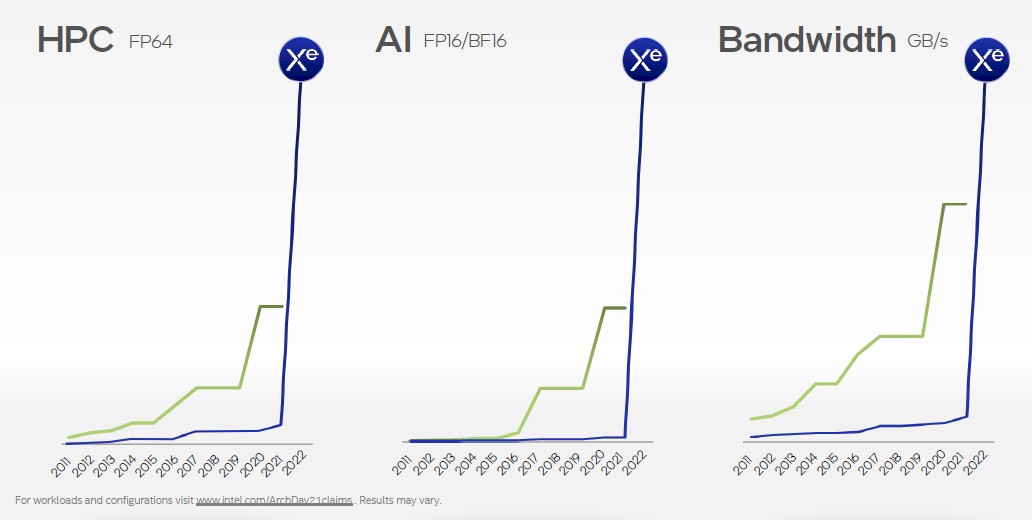
“We really wanted to close this gap in one shot, so we needed a moonshot,” Koduri continued. “We set for ourselves some very ambitious goals. We started a brand new architecture built for scalability, designed to take advantage of the most advanced silicon technologies. And we leaned in fearlessly.”
None of us believe the fearless part. Having delayed manufacturing techniques at the same time you are changing architectures is plenty scary. But being afraid should not be paralyzing, and swallowing its pride and moving to Taiwan Semiconductor Manufacturing Corp to make some of the elements of the Ponte Vecchio package has probably saved Intel’s efforts to be a real player in GPU compute. If Intel Foundry Services gets its manufacturing act together and has a decent price for etching chips, then it can regain that business. But Intel’s foundry cannot hold up Intel’s chip business ever again. This much is clear. Breaking the foundry out as chief executive officer Pat Gelsinger has done makes it accountable to the other parts of Intel as well as opening it up to co-design and manufacture chips for other companies, particularly those in the United States and Europe where it has foundry operations.
What is clear right now is that Intel needs a few successful moonshots to get itself back into contender positions in CPUs, GPUs, and FPGAs. The competition is pressing in on all sides. But if Ponte Vecchio is delivered early next year as planned, then Intel has a shot at getting its rightful piece of a new market.
The first test is the “Aurora” A21 supercomputer being installed at Argonne National Laboratory, which will have tens of thousands of these Ponte Vecchio GPU accelerators installed and representing the vast majority of the floating point processing power in the system, which was expected to have at least 1.1 exaflops and which is rumored to have 1.3 exaflops of aggregate compute. (Those are peak theoretical performance ratings.) This machine has been delayed a number of times, and its latest incarnation with a pair of “Sapphire Rapids” Xeon SP processors (possibly with HBM memory) and six Ponte Vecchio GPU accelerators was expected to make it onto the June 2021 Top500 supercomputer rankings so it would have some time on the list before the 1.5 exaflops “Frontier” hybrid CPU-GPU system based on AMD motors would take over on the November 2021 list. Here is an actual picture of the Aurora node:
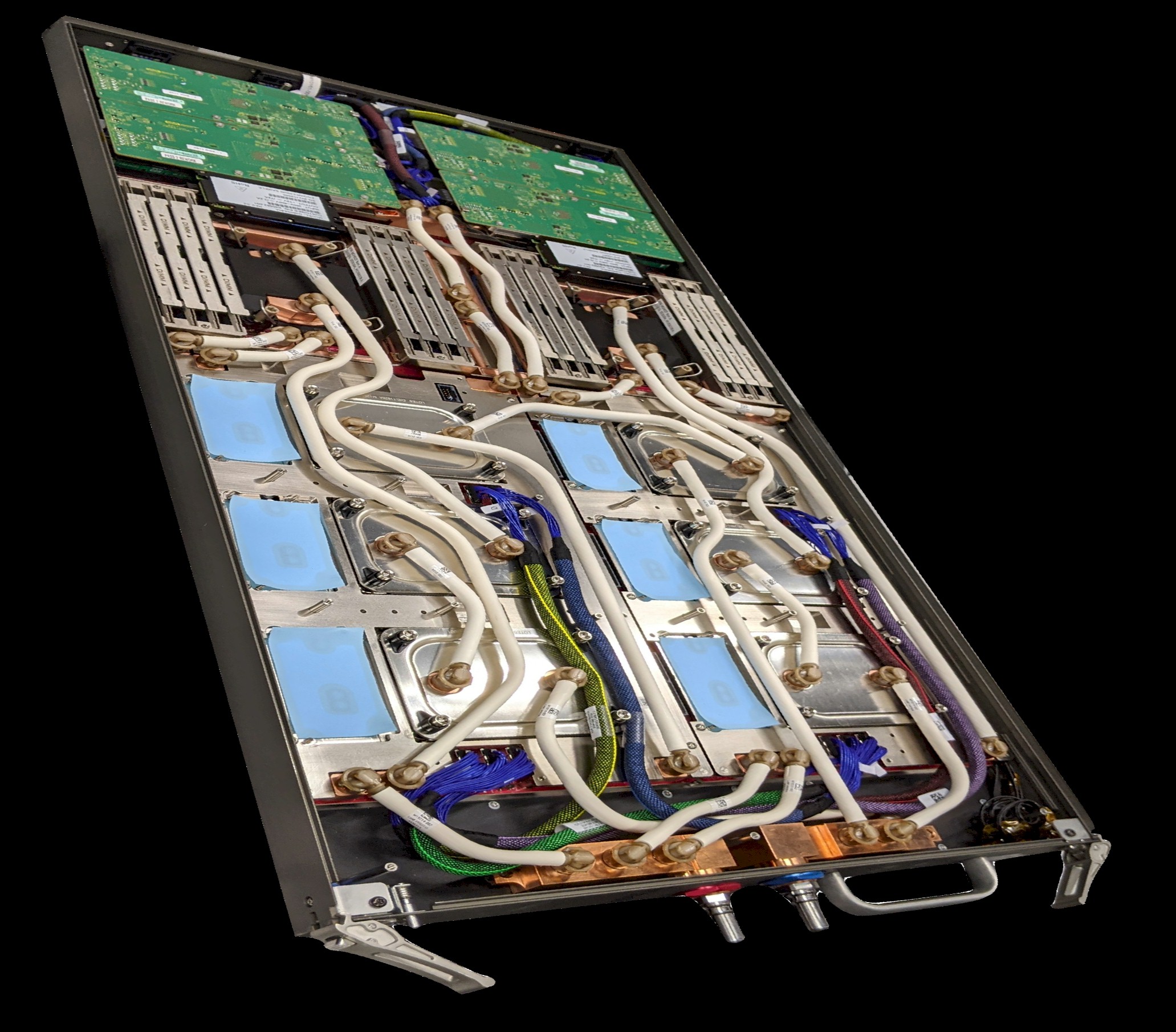
There is some chatter that the A21 node will use HBM2 memory on the Sapphire Rapids processors, and while this may be true – you can’t see the CPU in the picture above because it as been inverted in the two sockets in the back of the board – the A21 node clearly has eight DDR5 DIMM slots per socket. You can use both HBM and DRAM, and we would certainly do that if we were Argonne. Particularly if all of the HBM2 memory on the CPUs and GPUs can be clustered over Xe Link interconnects, as we suspect it can be.
Building Ponte Vecchio One Block At A Time
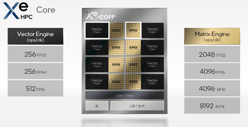
Being a parallel processor, a GPU accelerator can be assembled out of myriad compute elements that are wrapped up into bundles and then packaged and stacked to scale out its parallel performance. And that is precisely what the Ponte Vecchio Xe GPU does, as Hong Jiang, Intel Fellow and director of GPU compute architecture in Accelerated Computing Systems and Graphics Group, explained during his Architecture Day presentation. It all starts with the Xe core, which Intel calls Xe HPC Core, and it looks like this:
This is similar to the Xe cores used in other GPU variants created by Intel for normal laptops, normal desktops, gaming machines, or scientific workstations, but these have different compute elements and different balance of components and scale, just like CPUs do from Intel.
The Xe HPC Core has eight matrix math units that are 4,096 bits wide each and eight vector math units that are similar in concept to the AVX-512 units on the past several generations of Xeon SP CPUs. These are all front-ended by a load/store unit that can handle and aggregate of 512 bytes per clock cycle. That load/store unit is itself fronted by a 512 KB shared local memory (SLM) that acts as a L1 cache and also a separate instruction cache. We think that Intel is laying down FP64 units and FP32 units distinctly on the vector engine, much as Nvidia does with its CUDA cores on its GPUs. It looks like there are 256 of the FP64 units and 256 of the FP32 units on each vector engine, and then the FP32 units can be doubled pumped to deliver 512 operations per clock in FP16 mode. Yes, Intel could have just created an FP64 unit and carved it up into two or four pieces to get FP32 and FP16 modes, but this way, an intelligent, multitasking dispatcher can allocate work to two kinds of units at the same time. (As Nvidia has done with its GPUs for a while.)
The matrix math engines, which are roughly analogous to Tensor Core units in the “Volta” GV100 and “Ampere” GA100 GPUs from Nvidia, support mixed precision modes, including Nvidia’s own Tensor Flow (TF32) format as well as Google’s BFloat (BF16) formats in addition to the FP16 and INT8 formats commonly used in machine learning training and inference.
The vector engine thinks in 512-bit data chunks and the matrix engine thinks in 4,096-bit chunks at FP16 precision, it looks like.
The Xe HPC Cores are stacked up with ray tracing units – this is still a graphics card and will often be used for rendering and visualization in addition to compute, and within the same application often, which is a benefit – into what Intel calls a slice. Here is what an Xe HPC Slice looks like:
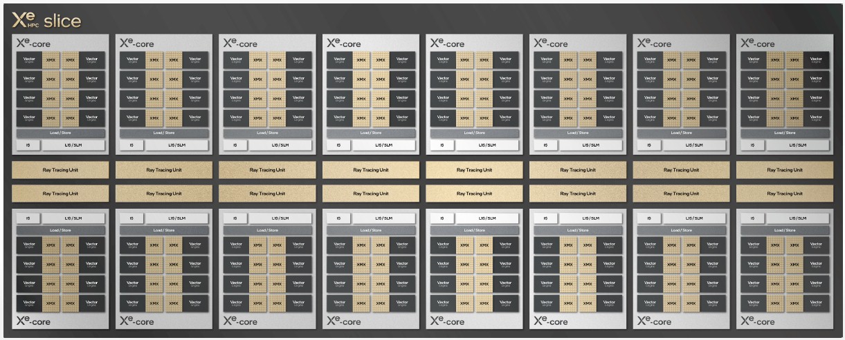
This particular slice has 16 cores and 16 ray tracing units paired one apiece to each core with a total of 8 MB of L1 cache across the slice. That slice has its own distinct hardware context inside of the Ponte Vecchio GPU complex.
An Xe HPC Stack is a complex comprised of four slices that has a total of 64 Xe HPC Cores and 64 ray tracing units with four hardware contexts, all linked to a shared L2 cache, four HBM2E memory controllers, a media engine, and eight Xe Link ports to connect out to adjacent GPU complexes for coherent memory as well as to CPUs that have Xe Link ports. Here is what the Xe HPC Stack looks like:
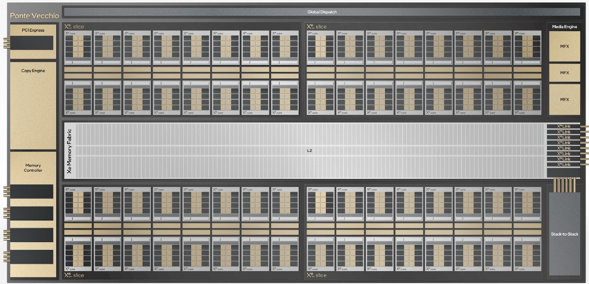
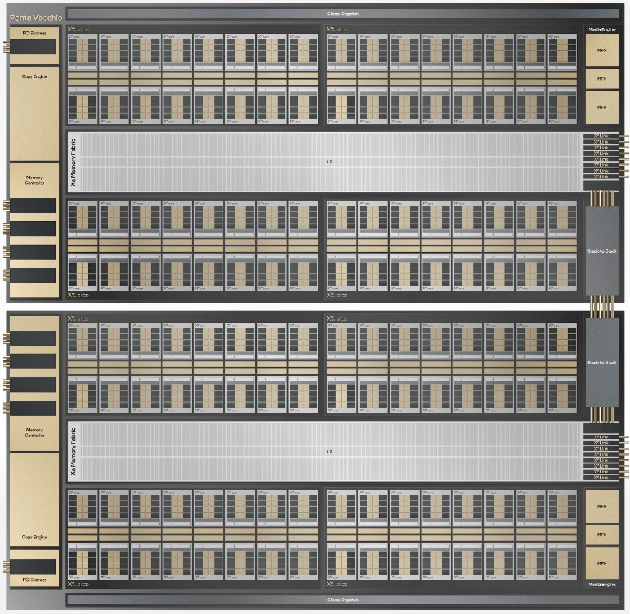
We strongly suspect that the Sapphire Rapids Xeon SP with HBM2E memory has Xe Link ports on it, and if it doesn’t, then it should. The Xe HPC Stack has a PCI-Express 5.0 controller on it as well as a copy engine, and the diagram shows three media engines, not one. Go figure. There is also a stack-to-stack interconnect that hangs off of the L2 cache memory for the stack, just like the Xe Links ports do. Think of this like NUMA interconnect for server chips where some NUMA links are local and some are remote. The stack-to-stack interconnect is for local links, presumably. It looks like Intel has a two-stack chiplet or chiplet complex, which is showed interlinked like this:
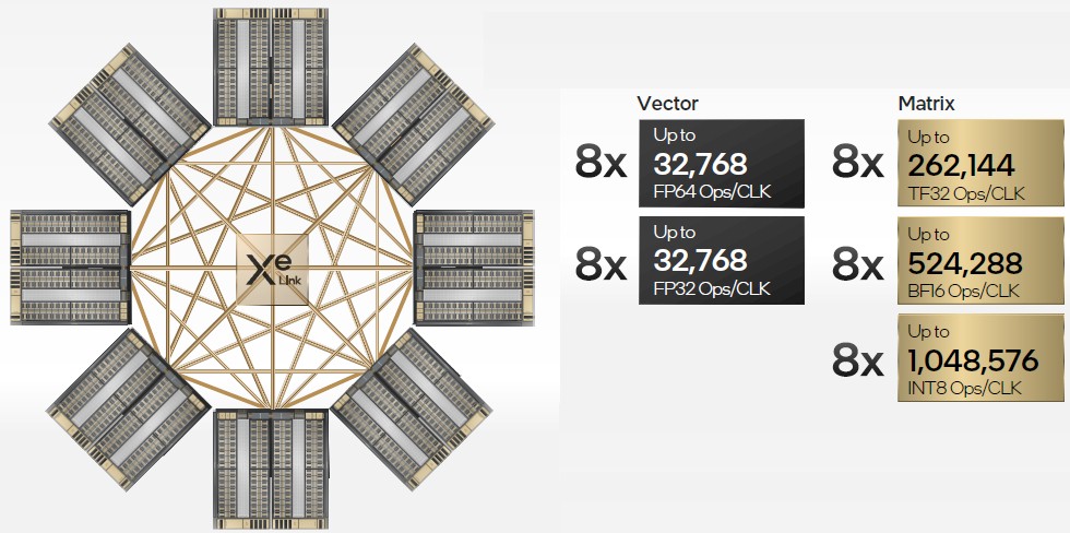
The Xe Link interconnect is interesting in that it includes high speed SerDes as well as a link fabric sublayer that is attached to a switch and a bridge that allows for up to eight Xe HPC GPUs to be interlinked gluelessly to each other with full load/store, bulk data transfer, and sync semantics across all eight GPUs. This Xe Link chip has 90 Gb/sec SerDes and an eight-port switch that has eight links per tile. It is etched using TSMC’s N7 7 nanometer processes.
As we said, we think the reason that the A21 node has only six GPUs is that two of the Xe Link ports in the Xe Link switch fabric are used to bring the two Sapphire Rapids sockets into the shared HBM2E memory complex. Anyway, here is what an eight GPU machine, where each GPU is comprised of two interconnected stacks, would look like in terms of its aggregate vector and matrix compute:
That diagram above is a statement of the possibilities of the Xe HPC architecture. Here is what the Ponte Vecchio device does to implement that architecture. First, here is the top view of the Ponte Vecchio package:
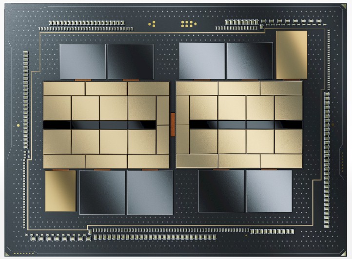
And then here is the exploded view that shows how EMIB and Foveros stacking comes into play to make these chiplets play together like one big monolith. Take a look:
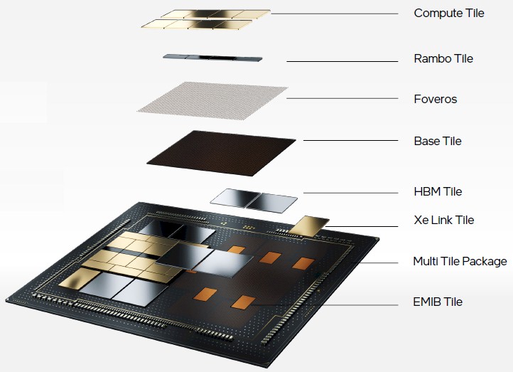
Each of the compute tiles shown at the top has eight Xe HPC Cores with 4 MB of L1 cache and a 36 micron bump pitch on the Foveros 3D stacking interconnect. These Xe HPC Core tiles are etched using TSMC’s N5 5 nanometer process, which started risk production in March 2019 and which ramped into production in April 2020. There are two distinct tile complexes on the Ponte Vecchio package, for a total of 128 Xe cores and 64 MB of L1 cache across those cores.
There are two base tiles, which have a PCI-Express 5.0 interface, 144 MB of L2 cache, and links to the HBM2E memory as well as EMIB interconnects between the eight Xe tiles. So the complete Ponte Vecchio complex has two PCI-Express 5.0 controllers and 288 MB of L2 cache. There are two HBM2E tiles, but we don’t know how much memory capacity they have.
The whole Ponte Vecchio complex has chiplets that employ five different process nodes of manufacturing across Intel and TSMC, a total of 47 chiplets, and over 100 billion transistors in the aggregate across those tiles. The A0 silicon (the initial stepping of the chip) has just been assembled, and it delivers more than 45 teraflops at FP32 precision, has more than 2 TB/sec of memory fabric bandwidth and over 2 TB/sec of connectivity bandwidth, according to Intel.
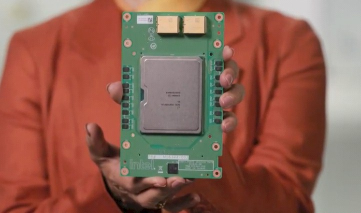
Intel is packaging Ponte Vecchio up in a form factor that looks familiar – it is the Open Accelerator Module form factor that Facebook and Microsoft announced two years ago. OAM will support PCI-Express and Xe Link variants, of course, and we can expect standalone PCI-Express cards as well even though Intel is not showing them. Here is the Ponte Vecchio package for real:
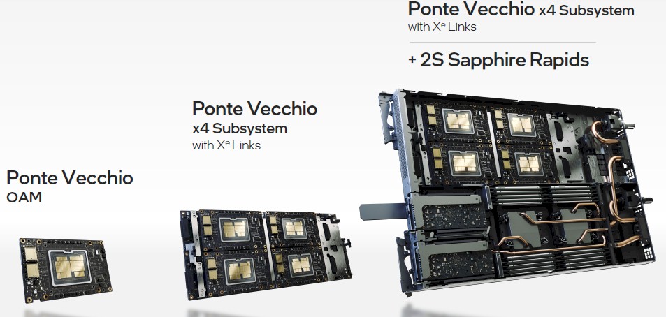
And here is some of the other server packaging options Intel has lined up aside from the six-way configuration being used in the Aurora A21 machine:
Before we can make any intelligent comparisons to Nvidia and AMD GPUs, we need to know if that is matrix or vector FP32 throughput for the device, and we need to know if Intel will have sparsity matrix support in its devices. We also need to know what it will cost. When we know these things, then we can make some real comparisons. And we are excited to do just that.


OSC Blends Intel HBM CPUs And Nvidia HBM GPUs For “Cardinal” Supercomputer
For a lot of state universities in the United States, and their equivalent political organizations of regions or provinces in other nations across the globe, it is a lot easier to find extremely interested undergraduate and graduate students who want to contribute to the font of knowledge in high performance …
Different GPU Horses For Different Datacenter Courses
If the semiconductor business teaches us anything, it is that volumes matter more than architecture. A great design doesn’t mean all that much if the intellectual property in that design can’t be spread across a wide number of customers addressing an even wider array of workloads. How many interesting and …

Covering All The Compute Bases In A Heterogeneous Datacenter
Intel has spent more than three decades evolving from the dominant provider of CPUs for personal computers to the dominant supplier of processors for servers in the datacenter. While Intel has argued that Moore’s Law is not dead – that the pace of innovation with transistors and therefore semiconductors has …
“We strongly suspect that the Sapphire Rapids Xeon SP with HBM2E memory has Xe Link ports on it, and if it doesn’t, then it should.”
David Blythe said, today in the hotchips presentation on Ponte Vecchio, that the connection between CPU and GPUs is PCIE … not CXL, and that Xe-Link has nothing to do with CXL.
Is the Rambo tile the L2 cache? Is there some other cache associated with the Xe-Link?