
Since Pat Gelsinger’s return to Intel as chief executive officer in early 2021, the company has bet big on bolstering its manufacturing processes and foundry business, expanded its fab footprint in the United States, and advocated for expanding the country’s chip making capabilities.
Intel’s success – or failure – in its foundry, and therefore in its own CPU and GPU businesses, depends on the scientists and engineers working out of the limelight in the company’s Components Research Group, whose work plays a key role in driving the evolution of Intel’s product portfolio. There are a few times every year where their efforts get put on display, such as at the Hot Chips show in August and this week at the IEEE’s International Electron Devices Meeting (IEDM) in San Francisco.
At the show, the group is presenting nine papers outlining technology being developed that will drive performance improvements and power efficiency in Intel’s silicon and Ann Kelleher, the chip maker’s executive vice president and general manager of technology development, will lead a plenary session December 5.
The papers also will highlight Intel’s continued drive to push forward Moore’s Law debates within the industry whether the decades-old observation that has steered the direction of the tech industry since 1965 is running out of steam.
Some of the technologies that have made their way from Components Research into silicon include strained silicon (to reduce heat), high-k metal gates (power consumption), FinFET (performance), and last year, RibbonFET (power consumption), and PowerVia (power efficiency).
“These all took their first breath of life within the walls of Components Research,” Paul Fischer, director and senior principal engineer in Components Research, told journalists and analysts during a pre-IEDM briefing. “Packaging innovations as well, like EMIB and, more recently, Foveros Direct.”
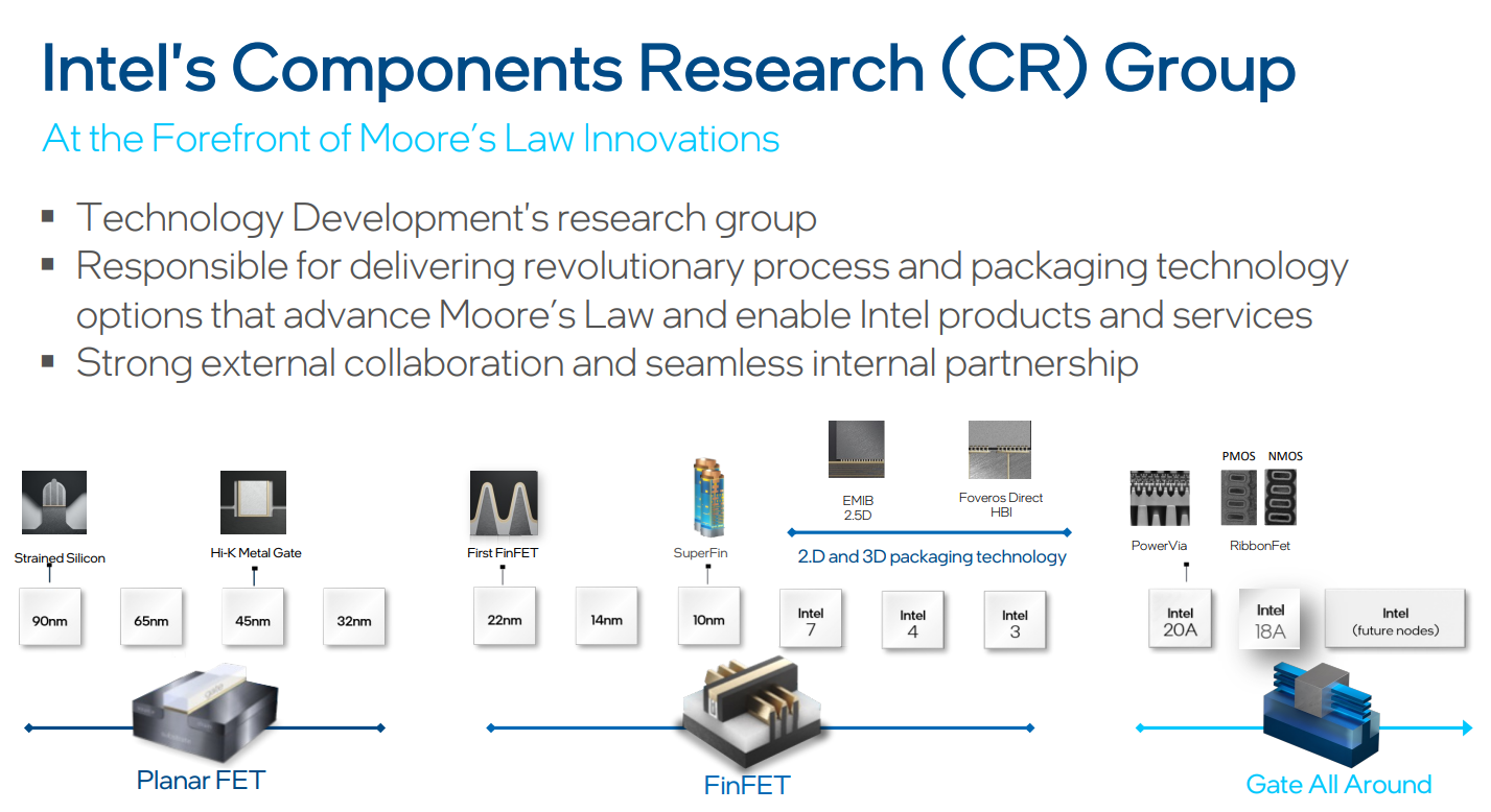
Fischer placed the technologies that will be talked about in the papers into three categories: 3D packaging to drive the integration of chiplets, 2D materials for scaling transistors, and power efficiency and memory advances to improve performance.
In the first bucket, Intel will talk about quasi-monolithic chips, which Fischer described as “harnessing new materials and processes which are in exciting ways starting to blur the line between where silicon processing ends and packaging begins” that is driving a 10X improvement in interconnect density over what Intel introduced at last year’s IEDM. Intel in 2021 showed the results of its first work in hybrid bonding scaling reaching 10 microns, he said. Quasi-monolithic chips drives that to 3 microns.
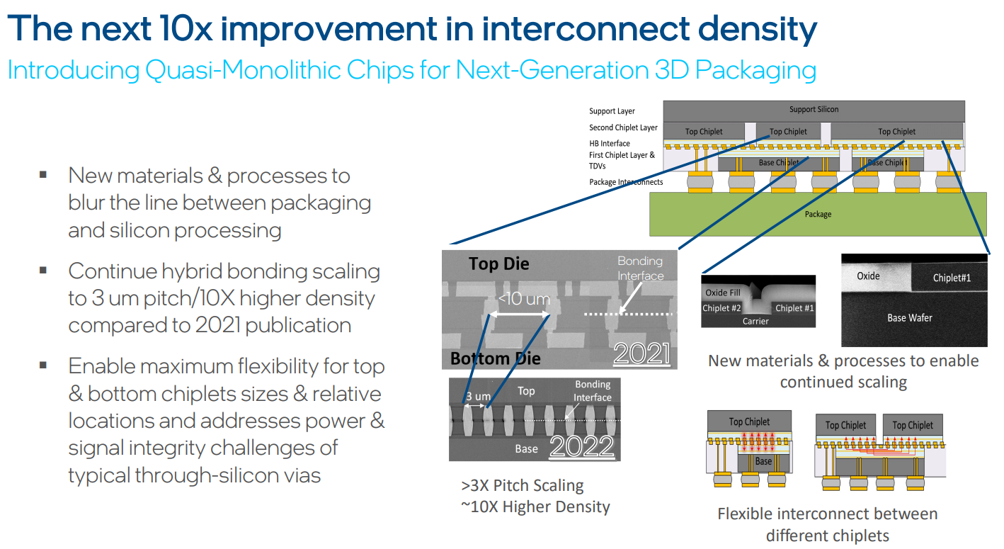
“If you take that into two dimensions, that gives you the 10X density improvement,” Fischer said. “This is all over and on top of the 10X in density improvement we talked about last year. So in a mere couple of years, we’re talking about 100X total cumulative improvement in interconnect density. It’s a remarkably fast rate of change.”
The quasi-monolithic chip design also provides greater flexibility when it comes to chiplets, including where they can go, what sizes are possible, and how many stacks of chiplets can be incorporated. “It creates a very flexible opportunity for us to then stitch together these chiplets with fidelity of interconnects that are comparable to the same fidelity of interconnects we can achieve as if they were … fabricated monolithically on die,” he said. “Hence, that’s why the team is calling these quasi-monolithic chips.”
The Component Research group also is working on 2D materials that Fischer said will enable Intel to fit more transistors onto a single chip and keep Moore’s Law moving forward. Most semiconductor materials – silicon, gallium nitride, and silicon carbide, for example – depend on a three-dimensional crystal, with atoms bonded in all three dimensions. With 2D materials, all the bonds are done in one place.
Intel has shown a gate-all-around (GAA) stacked nanosheet structure using 2D channel material that is 3 atoms thick. At the same time, the company reached near-ideal switching of transistors on a double-gate structure at room temperature with low-leakage current. Both capabilities are essential for stacking GAA transistors, which will push the industry beyond limits imposed by silicon, Intel said.

“That’s critical as we think about scaling of transistors,” he said. “It’s the channel thickness that has to scale commensurately with the X and Y as well. You need all of those dimensions to scale these materials. That’s why they’re so attractive for the industry and certainly at Intel.”
Another challenge with 2D materials is making electrical contact because of how thin they are. Intel is developing models to help understand the physics needed to make the electrical contacts to 2D materials. The researchers have created a comprehensive analyst of electrical contact topologies to 2D materials, which could lead to high-performing and more scalable transistor channels.
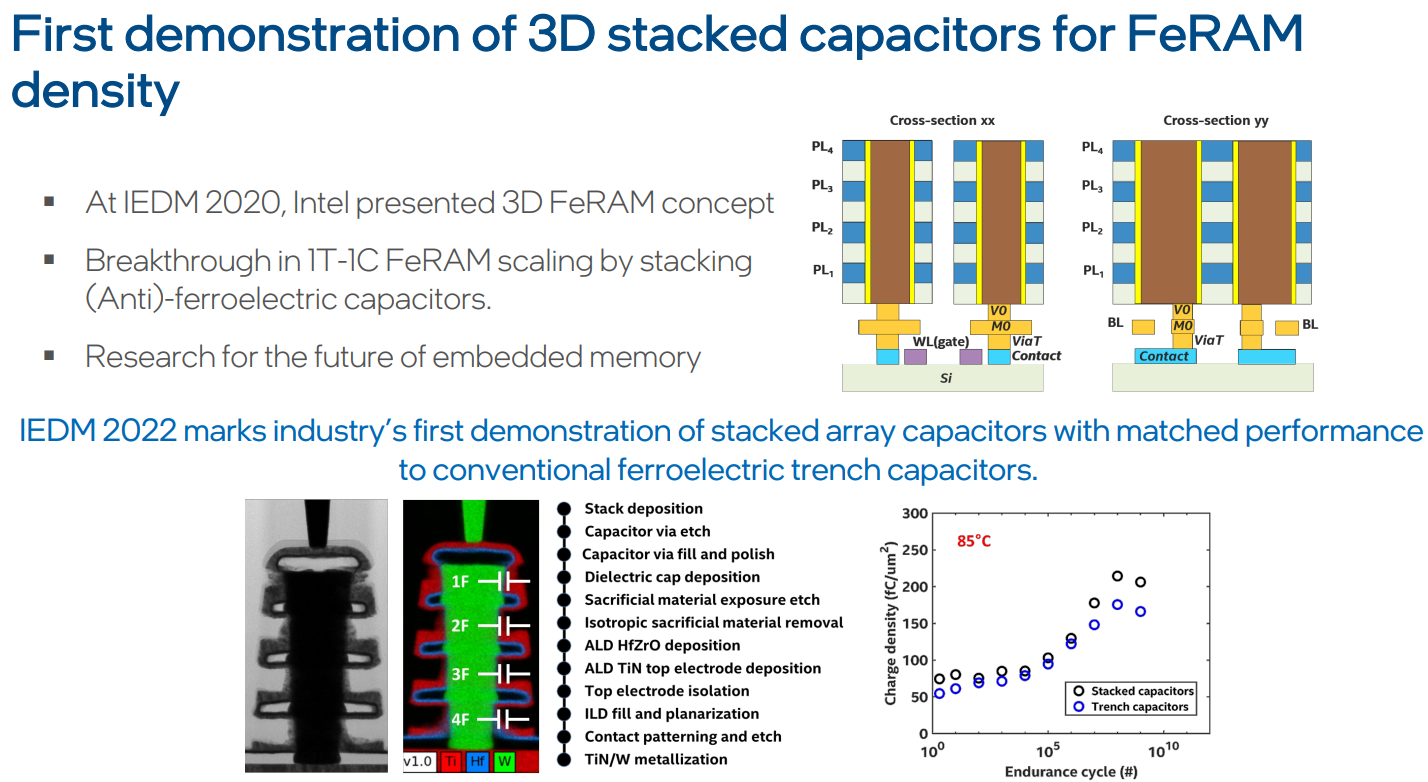
For better power efficiency and memory, Intel two years ago introduced the concept of 3D stacked ferroelectric memory.
“We believed that this was possible,” Fischer said. “A unique attribute of ferroelectric materials is the fact that the charge is fixed. Within one trench or one via, we can actually create a number of different individually identifiable addressable capacitors and that’s fantastic because it’s a path towards density scaling, using one widget and creating four storage elements out of it. It’s a very exciting concept. Ideas are easy. The demonstration is hard.”
This year, the company is demonstrating it, showing stacked ferroelectric capacitors that offer the same performance of conventional ferroelectric trench capacitors and using them to build FeRAM on a logic die, Intel said.
The researchers also developed a device-level model to improve ferroelectric hafnia devices by showing mixed phases of states and defects, which could help lead to the development of new memories and ferroelectric transistors. They’re also looking beyond 5G while address power efficiency by working toward 300-millimeter gallium nitride (GaN)-on-silicon technology, which could deliver a 20-times gain over industry-standard GaN.
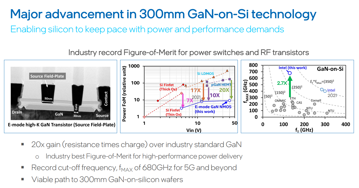
Intel is adding a source-connected steel plate in the transistor design, which “has enabled us to demonstrate a 20X gain and a key figure of merit for power delivery,” he said. “So best-in-class devices with 20X gain in a key figure of merit for power delivery. That same transistor architecture has enabled us to demonstrate and measure record cutoff frequencies, which is a critical figure of merit for communications. This would be fantastic for applications in 5G and beyond.”
In addition, the researchers are working to reduce the operating voltage to increase power efficiency. Devices today typically operate in the 0.6 volts range, due to the physical properties of the semiconductors for switches, Fischer said. The Components Research group is showing low-voltage and high-speed switching of a magneto electric device.
“They’re using lanthanum-doped bismuth iron oxide as a sterile electric material,” he said. “By applying an electric field across that, they’re able to switch the magnetic moment to the material and it is in a permanent state until another potential is applied. You can switch it back by applying a mere 150 millivolts. They’re able to switch that state and that would be a critical opportunity to reduce the operating voltage. Imagine a switch that works at 150 millivolts as opposed to .6 volts.”
This is important because the device’s energy is proportional to the square of the voltage, according to Fischer. In addition, it’s key that these materials can switch at high speed. With relatively large devices – about four square microns – the researchers have demonstrated a switching speed of 2 nanoseconds.

Industry Behemoths Back Intel’s Universal Chiplet Interconnect
When the hyperscalers, the major datacenter compute engine suppliers, and the three remaining foundries with advanced node manufacturing capabilities launch a standard together on Day One, this is an unusual, significant, and pleasant surprise. And this is precisely what has happened with Universal Chiplet Interconnect Express. The PCI-Express interconnect standard …

Intel’s “Ponte Vecchio” GPU Better Not Be A Bridge Too Far
It is pretty obvious to everyone who watches the IT market that Intel needs an architectural win that leads to a product win in datacenter compute. And it is pretty clear that the top brass at Intel are putting a lot of chips down on the felt table that the …
Chip Makers Press For Standardized FP8 Format For AI
In March, Nvidia introduced its GH100, the first GPU based on the new “Hopper” architecture, which is aimed at both HPC and AI workloads, and importantly for the latter, supports an eight-bit FP8 floating point processing format. Two months later, rival Intel popped out Gaudi2, the second generation of its …
“in its foundry, and therefore in its own CPU and GPU businesses”
Intel is building its ARC GPUs at TSMC. Also the compute tiles of its MAX GPUs. I believe they’ve also announced that the Meteor Lake tGPUs are TSM N5. Looks to me like they can compete without their own foundry on GPUs.