The need for speed to process neural networks is far less a matter of processor capabilities and much more a function of memory bandwidth. As the compute capability rises, so too does the need to keep the chips fed with data—something that often requires going off chip to memory. That not only comes with a performance penalty, but an efficiency hit as well, which explains why so many efforts are being made to either speed that connection to off-chip memory or, more efficiently, doing as much in memory as possible.
The advent of 3D or stacked memory opens new doors, especially for those with deep learning workloads. We have already talked about how memory is the next platform for machine learning, and have explored a number of architectures that seek to maximize on-chip memory by making it handle at least some of the compute via accumulation engines. Among such approaches we have explored are the Nervana Systems architecture, Wave Computing’s hardware for deep learning, and other research efforts, including Neurocube, which leverages 3D memory and accumulators to boost neural network processing.
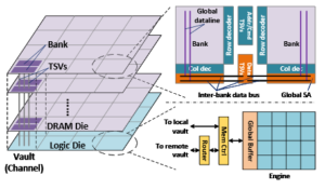
Building off the Neurocube research architecture (from Georgia Tech) is a more expanded hardware and software stack that uses 3D memory as the springboard for neural network. The chip project, TETRIS, is a 3D memory-based processing approach cobbled together by Stanford researchers that takes aim at the memory bandwidth problem presented by existing architectures by adding more capabilities inside the stacked memory cube—in this case Hybrid Memory Cube (something we described in detail in a larger discussion of the Neurocube approach).

When it comes to attacking the performance and energy efficiency bottlenecks of moving data to and from off-chip memory, one approach has been to use larger on-chip SRAM buffers that can keep much of the data in cache for reuse. While this works, it’s an expensive solution since it increase the chip area and makes all operations less efficient. The team behind TETRIS subverts this by rebalancing the resources between the computation and those buffers. Since 3D memory has higher bandwidth, the energy requirements are lessened and there is no need for larger buffers. Even when TETRIS added more computing elements into the mix and provided fewer buffers, they were able to capture a 40% improvement in performance and energy compared to the large buffer approaches.
As one of the TETRIS leads, Mingyu Gao, tells The Next Platform, “We also found we could use smaller buffers as an option, but one issue with this is that the off-chip accesses may increase because larger buffers can cache more data on the chip, but if you reduce the buffer, you have more changes of going off-chip.” He says they tried to leverage some of the recent advances in in-memory accumulation and near-data processing (which has been the subject of Gao’s research for a number of years) to push the larger computations into memory. “We put a very simple accumulation logic unit into the chip, so instead of fetching the data and adding values onto that and storing it back, we just pushed it to the memory.” The result, like the fix, is deceptively simple—this addition of an accumulation unit means there is one direction of traffic versus round-trip traffic—a 2X improvement in performance and efficiency.”
The interesting thing here, beyond how clean and easy this seems, is that this appears to be the trend for startups targeting the deep learning market with novel arcitectures. While we have only been able to garner some details about Nervana, Wave, and others, this in-memory computation inside of 3D memory is the major differentiator—and if the research results from what is publicly known are any indicator, these speedups and efficiency gains are nothing to dismiss. However, where the real technical challenge lies is in getting the scheduling and other software elements to play nice with this. Gao says he thinks the TETRIS team at Stanford has found a suitable solution.
Another interesting twist the TETRIS team implemented was using the multiple memory channels available on stacked devices to create a parallel engine—one compute element can be associated for each of these channels for faster parallel performance. This is where the hardware speedup was most clear, but of course, the software dance had to be refined, especially in terms of scheduling to control the order of computations (not all data can be buffered on chip, so finding the optimal ordering to minimize off-chip data access is a big challenge). With the 3D memory and smaller buffers, the problem shrinks, Gao explains, and their analytical model to this optimization problem saved on overall energy efficiency as well as compared to exhaustive search across a global model.
In terms of choosing HMC for TETRIS, Gao says there are hardware similarities across everything that has been proposed, but the real HMC differentiator was the interfacing capabilities with HMC.
As with the other architectures we have cited here, there is still a long way to go to get such chips to market, especially given the lack of availability of 3D memory technology to the wider market. However, Micron and others are working to push 3D memory into research centers to spark the next wave in chip design—one that is no longer encumbered by the same memory bandwidth restrictions.


Be the first to comment