

We have heard about a great number of new architectures and approaches to scalable and efficient deep learning processing that sit outside of the standard CPU, GPU, and FPGA box and while each is different, many are leveraging a common element at all-important memory layer.
The Hybrid Memory Cube (HMC), which we expect to see much more of over the coming year and beyond, is at the heart of several custom architectures to suit the deep learning market. Nervana Systems, which was recently acquired by Intel (HMC maker, Micron’s close partner), Wave Computing, and other research efforts all see a common need—and solution.
For deep learning workloads, the compute is not as central as pushing a great deal of data, much of it which can be reused, through the system. While FPGAs and GPUs and even some CPUs can all handle such workloads, at the end of the day, the performance per watt on specialized deep learning approaches is what will be the game changer—at least according to the few companies that are dipping toes into these fresh waters. The goal is to leverage the logic layer inside the HMC with tailored multiplier and accumulator capabilities to preserve the high memory bandwidth and lower energy consumption, which is what many of the startups in the new area of deep learning chips have discovered, albeit via different paths.
To be fair, HMC is not the only 3D memory option and in fact, it will not be the first stacked memory approach finding its way onto new systems. The Pascal GPU architecture features High Bandwidth Memory (HBM) which is an effort backed by AMD and others. HBM offers an alternative to the Intel and Micron partnership, which is valuable for Nvidia in its rivalry with Intel, especially when it comes to the emerging deep learning market—one that Nvidia had a head start with and now has Intel nipping at their heels. What is different about what Nvidia will do with Pascal is that the logic layer and its custom functions are not the central piece—the challenge for the GPU maker will be making scalable systems that can leverage HBM. For many deep learning chip startups, and research efforts such as NeuroCube, which will get to in a moment, the emphasis is at the single HMC device level. Scalability of such devices is possible (unless a NUMA-like capability is required) but for now, offers its own suite of barriers.
Wave Computing, Nervana Systems, and others have described the memory bandwidth challenges for offload architectures and the flexibility of reprogramming for FPGAs in the past. However, we have only been able to delve into limited architectural detail with both companies given their need to preserve the secret sauce that makes their chips scalable, low-power, and high performance for deep learning frameworks. An effort out of Georgia Tech called NeuroCube, however, sheds a bit more light on what is possible on top of the existing logic layer in HMC in particular.
While we cannot explicitly say that NeuroCube replicates what the other companies producing HMC-based deep learning architectures are doing, looking at the concept in closer detail shows how HMC itself is a key enabler for workloads that could benefit greatly from the reprogrammability of an FPGA and the performance of a GPU but at a lower performance price. As one of the lead architects of NeuroCube, Saibal Mukhopadhyay, tells The Next Platform, there is a middle ground between the value propositions of custom ASICs (which aren’t flexible), FPGAs which is limited in the number of neural networks that can be handled at runtime, and GPUs, which work well but are not as power efficient. “We wanted to design a neural computing platform which could be software programmable and could be programmed to have different types of networks but with power efficiency numbers that are close to a custom ASIC.” The real problem for any architecture outside of flexibility and power efficiency, he says, is memory bandwidth. The natural place to start is with a high bandwidth memory approach, in this case HMC (not HBM because the team already has a relationship with Micron and Intel, Mukhopadhyay says).
Although much of the material about NeuroCube puts the effort in the neuromorphic computing category, this is a different way of thinking about neuromorphic computing. Many tend to think of such devices as based on IBM’s True North architecture or other biophysical-inspired “spiking” models. This is different—it is more a generalized neural network for convolutional and recurrent neural networks primed inside the logic layer of the HMC and programmable at runtime.
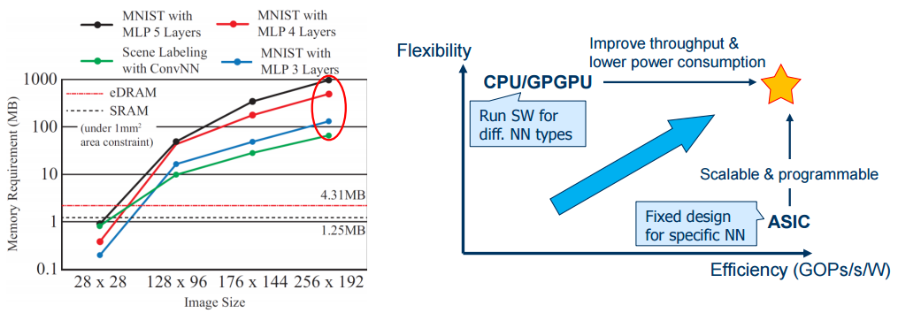
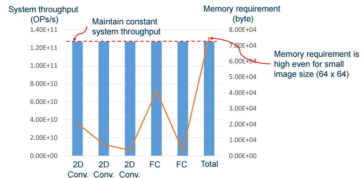
To highlight the programmability, performance, and power tradeoffs of custom ASICs, GPUs, and CPUs, and show the need for memory, Mukhopadhyay shared the following graphic. For the operations shown on the left, the amount of memory needed is far more than can be stored on-chip but the computations are quite simple, requiring just a multiplier and accumulation capability (no floating point—again, back to the low-precision/fixed point argument). The design of this “neuromorphic” platform has simple embarrassingly parallel operations but is limited by the ability to get the large amount of data into the chip.
The Georgia Tech team’s “programmable digital neuromorphic architecture with high-density 3D memory” addresses this in two ways. First, by bringing the logical compute layer for math operations into the memory stack where there is already a layer (see yellow section). Therein is the “vault controller” which pushes data from DRAM to a tiny CPU and do all of this while meeting the thermal and area constraints of the DRAM (currently at 28nm but the team found they could handle 5GHz at 15m maximum before frying the DRAM).
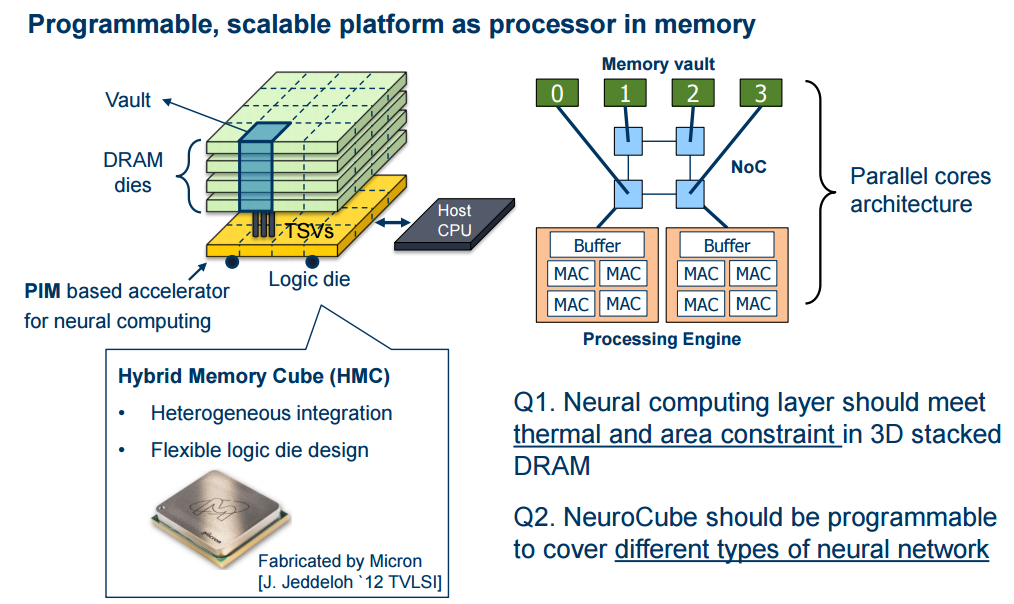
Below you can see the host CPU (which just sends numbers to the NeuroCube to help it decide what type of neural network is being run; it also pushes the data to the DRAM and handles that write and the results). All computation is being done on the logic area inside the HMC, which will be multiple cores with buffers, multiply, and accumulate engines that fit into the yellow space.
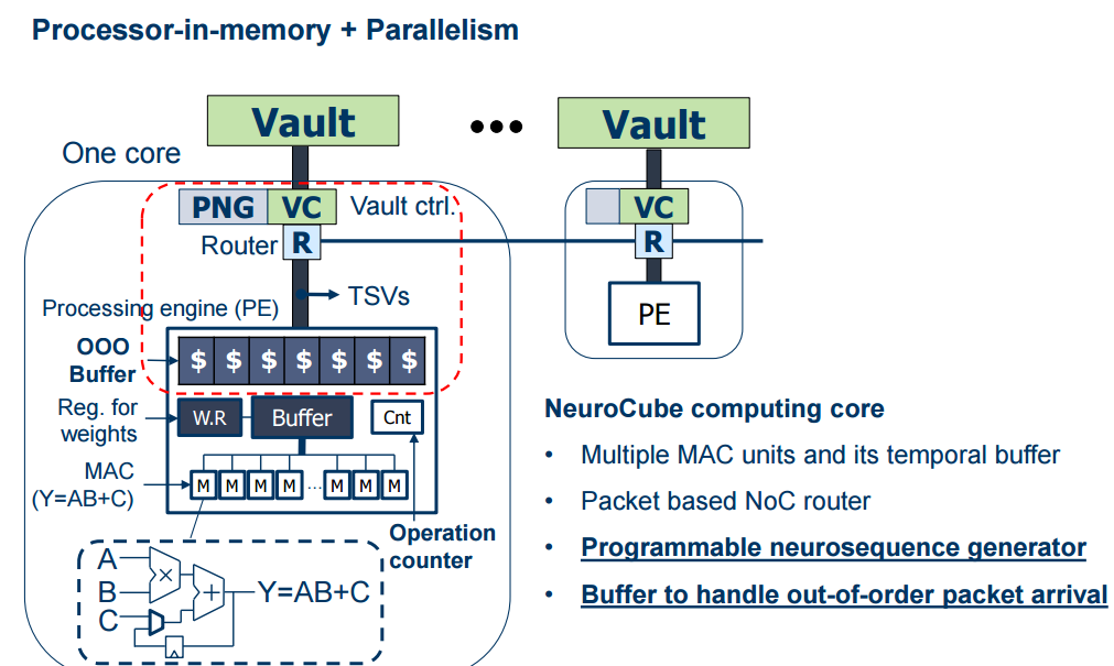
A closer look at the layer inside the HMC reveals a simple architecture for what are really quite simple math operations—just the concept that has spurred deep learning chip startups to circumvent existing general purpose architectures with their emphasis on floating point and lack of ultra-fast memory bandwidth and added latencies.
As a side note, since the HMC architecture already exists (although not in systems yet) with that logic layer—and since the Georgia Tech team has shown these capabilities can be added without cooking or outsizing the DRAM, there is nothing but a lack of market interest preventing Intel and Micron from designing and fabbing such a chip—if they aren’t already planning to do so with the Nervana IP they acquired.
It is not difficult to see how Intel and Micron might spin out such an effort or how other startups might not try to do something similar with HBM (which has a similar logic layer—there is nothing preventing this from happening on HBM and in fact, cooking more into the logic layer is part of ongoing work at AMD via a Fast Forward project). But of course, the fatal flaw of all architectures that can solve a problem really well is always programmability. This design, which has thus far only been implemented on FPGA (the host CPU on the above slides is the simulated part) has two parts programming-wise that show an advantage over other approaches like FPGAs (not runtime programmable) or ASICs (which can only be programmed for one logic function at a time). This is software programmable, like a GPU, which opens it up to more users potentially.
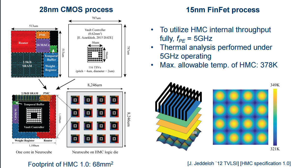
So, how do these perform based on simulation results? First, take a look at how the hardware holds up at 5GHz (a critical numberbecause that’s the rate the data can come into the logic layer) at both 28nm and 15nm.
With the above in mind, look at the hardware breakdown of simulation results below.

Below, see results for training on the original digit (handwriting) recognition workload, based on simulation results at 15nm FinFET
“We have four HMC devices in our lab connected in a backplane, Mukhopadhyay says. “We have a vision for connecting these into a cognitive solver but the challenge is different. Scaling at this level is a different algorithmic and architecture question. The larger the network, the more connected machines are needed. We can explore it, but the question becomes how to virtualize such a network across these cubes.”
This scalability of devices is what Wave Computing, Nervana Systems, and other startups have either solved or are trying to do with their machines—it will be interesting to see what the limitations are from the hardware side and how these outpace what is possible in software.
Full slide deck can be found here. Interestingly, it is not missing some results that were shown prior to our interview comparing various low-end Nvidia GPUs, including Tegra for performance/power comparisons. Hope to see those re-appear sometime soon or updated with more deep learning-specific GPUs than mobile/desktop versions (i.e. M40/M4, Pascal, TitanX, etc).

He Who Can Pay Top Dollar For HBM Memory Controls AI Training
What is the most important factor that will drive the Nvidia datacenter GPU accelerator juggernaut in 2024? Is it the forthcoming “Blackwell” B100 architecture, which we are certain will offer a leap in performance over the current “Hopper” H100 and its fat memory younger sibling, the H200? No. Is it …
What Faster And Smarter HBM Memory Means For Systems
If the HPC and AI markets need anything right now, it is not more compute but rather more memory capacity at a very high bandwidth. We have plenty of compute in current GPU and FPGA accelerators, but they are memory constrained. Even at the high levels of bandwidth that have …
How High-Bandwidth Memory Will Break Performance Bottlenecks
Intel recently announced that High-Bandwidth Memory (HBM) will be available on select “Sapphire Rapids” Xeon SP processors and will provide the CPU backbone for the “Aurora” exascale supercomputer to be sited at Argonne National Laboratory. Paired with Intel’s Xe HPC (codenamed “Ponte Vecchio”) compute GPUs running in a unified CPU/GPU …
Wow very interesting concept. I really could see Micron jumping on this as they are looking for new ways to extend their memory architecture and that one clearly looks like a very interesting potential target. GPUs will eventually loose the race as they have the same problem as CPUs they need to cater to different applications area. Unless they specialize in a particular area so make a specific design choice for one application area they going to be left out in the cold. Intel acquiring more and more IP will eventually just slack some component onto their CPU die and it makes sense for them makes far less sense for GPUs
Your comments on the Internet are consistently about Intel > Nvidia since last year. Are you longing INTC and shorting NVDA? Seems pretty obvious
So its been shown (to my surprise) over the past few years that GPU:s are even more energy efficient than FPGA:s at running AlexNet, 24 images / s / watt on Tegra X1 and ~12 images/s/watt on Altera…
And here Nicole is claiming that FPGA:s are more efficient without any evidaaannce ? Girl please 🙂
Not my claim, the statement of the project’s authors with benchmarks to support in the paper. Sharing data as I get it.