

We can talk about storage and networking as much as we want, and about how the gravity of data bends infrastructure to its needs, but the server – or a collection of them loosely or tightly coupled – is still the real center of the datacenter.
Data is useless unless you process it, after all. As more than a few companies that have built data lakes as a knee jerk reaction have come to realize.
The server is where organizations spend the bulk of their budgets when they build platforms – excepting, of course, the vast sums they lavish on writing or procuring their applications. We are old enough to remember when what happened in glass houses was called data processing, not the more vague information technology, and we would point out that what the industry calls a datacenter should, properly speaking, probably called a data processing center.
We are not snobs about the computing aspects of data processing here at The Next Platform, and we are certainly not prejudiced against storage or networking as is attested in our broad and deep coverage on all three aspects of a modern system. We are well aware of the fact that moving data from the slowest storage tiers of tape cartridges and disk drives up through networks and main memory and caches in the system out to the central processing units of servers is one of the more complex engineering dances ever orchestrated by humanity. And we suspect that very few people can see an entire system in their heads, even if they built them.
The View From Outside The Glass House
It is fun sometimes to just step back and really consider how complex something like a banking application or a weather simulation or a social media network serving over a billion and a half people truly is. And if you really want to blow your mind, try making the connections between systems within companies and then connections across companies and consumers over the Internet. Perhaps the only accurate metaphor, given this, is to call the entire Earth a data processing center. Any alien looking down from the outside of the atmosphere would clearly see that humanity is on the cusp of adding intelligence to the automation systems we have been gradually building since the advent of computing in the wake of World War II. It started with card-walloping mainframes doing bookkeeping and it is evolving into a massively sensored and, at some emergent level that might be short of consciousness we hope, self-regulating systems.
And still, beneath all of these layers and behind all of these interconnections, at the heart of it are some 40 million servers, chewing on all that data as their applications make the economy dance or entertain us with myriad distractions.
As we look to new processing, storage, and interconnect technologies and the architectures that will weave them together into systems, we can’t help but wonder if the servers that enterprises buy in a year, or two, or three will bear much of a resemblance to the ones they are accustomed to buying today. Many have predicted radical shifts in the past, and some occurred, such as the rise and ubiquity of X86 machines and the fall of proprietary minicomputers and Unix systems in the datacenter. And some have not. The advent of wimpy-cored microservers or the demise of the mainframe come to mind. Prediction is almost as difficult as invention.
We will be talking to experts over the course of this series of stories, and we are merely setting the stage here for those experts to speak, much as we did last year with the Future Systems series we did relating to high performance computing architectures. (See the bottom of this story for the Related Items section for links to those articles.) We will start with some general observations about the core components of the server and the general trends for their innovation, and we welcome your input and comments as this article series evolves.
Processors
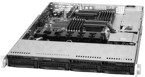
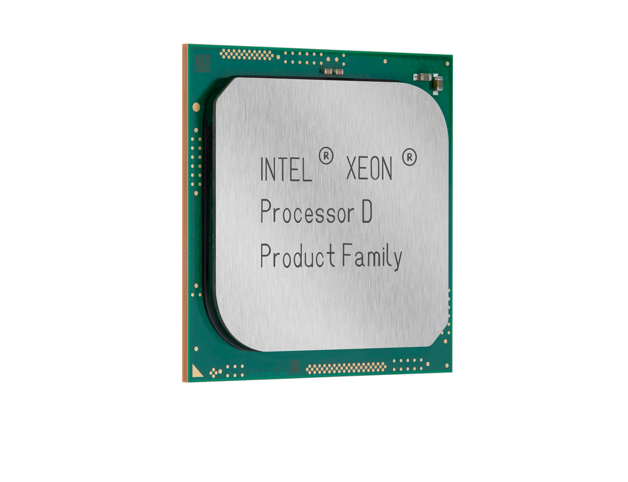
It is not much of an exaggeration to say that a modern processor socket looks like a complete multiprocessing system implemented in silicon with main memory and other forms of storage externalized. Multicore processing came to RISC processors in 2001 beginning with the Power4 chip from IBM, and Sun Microsystems and Hewlett Packard followed suit. Intel got its first dual-core Xeons into the field in 2005, and since that time not only has the company done major microarchitectural shifts, such as adopting cores aimed at laptops in its servers, but it has ramped up the core count while at the same time bringing PCI-Express peripheral controllers and Ethernet networking interfaces onto the processor itself. With the Xeon D chips, Intel is bringing the chipset that links to peripherals (called the southbridge) onto the package, and it won’t be long before FPGA accelerators will be brought onto the die. (We think this might also be with a Xeon D chip that was created for hyperscalers, but that is just a guess.)
Here we are, at the dawn of the “Broadwell” Xeon v4 generation, where E5 processors will have up to 22 cores and E7s will have up to 24 cores according to the Intel roadmaps that The Next Platform got ahold of last May, we are starting to run out of processing increases coming from increasing core counts much as we hit the clock speed wall back in the early 2000s that led us down the road to multicore chips in the first place. And with the “Skylake” Xeon v5 generation, it looks like Intel will push the core count of the top bin processors up to 28 cores, according to those roadmaps, with all kinds of innovations wrapped around them. The cores are getting moderately faster with each generation, too, and the floating point performance has been much more radically increased as well in recent Xeon generations, but it is hard to imagine software that will be able to harness all of the compute in systems beyond that and future servers would seem to be ideal for workload consolidation but in terms of raw processing per thread, we cannot expect much in the way of performance increases. We will have to juggle more work across more threads and drive up utilization, and the threads will only get faster at a nominal rate between generations on the order 5 percent to 10 percent.
There are only a few other CPUs that matter in the datacenter. A handful of ARM chips from upstarts like AMD, Applied Micro, Broadcom, Cavium, and Qualcomm, some of which are starting to ramp now but none of which has scored a big win yet that can count as a tipping point in the server market. IBM’s Power8 chip is trying to follow ARM with a licensing and proliferation approach, and is counting on adoption in China to drive volumes much as the ARM collective is doing. The ARM collective is hoping to capture 25 percent share of server shipments by 2020, and IBM’s top brass similarly aspire for the OpenPower platform to attain 10 percent to 20 percent market share. These are both lofty aims, and both camps are depending on heavy adoption in China, which is facing a number of economic challenges at the moment. The Sparc processors from Oracle and Sparc64 chips from Fujitsu still count, too, and by 2017, AMD will have its “Zen” CPUs in field as well, if all goes as planned.
But for now, the motor of choice for compute is the Xeon E5 processor and it is the one to beat. This is Intel’s market to lose, and it will take something truly radical to alter the market dynamics here. Intel is not exactly sitting still. Interestingly, Intel is positioning its future “Purley” platforms using the Skylake Xeons to consolidate the Xeon E5 and Xeon E7 lines to simplify server design for OEM and ODM partners and as well as customers who craft their own gear. The Purley platforms using Skylake Xeons will scale from two to four to eight sockets all with one processor family, socket design, and memory architecture, which has not been the case before. The Xeon E7s have had a different socket and memory design, and while this has added performance and scale, it has added costs. Intel has figured out how to accomplish its scale and reliability goals with a single, unified Xeon line, according to the roadmaps we have seen, which should make it all that more difficult for those peddling four-socket and larger systems to afford their differentiation. Intel will be working with third parties – presumably Hewlett Packard Enterprise, SGI, and NEC – to offer scalability beyond eight sockets for these future Skylake Xeons.
Aside from all of that, it is amazing to ponder just how much work a two-socket Xeon server with 56 cores and a few terabytes of mixed DRAM and 3D XPoint memory plus flash drives linked by NVM-Express links will be able to do. The node counts in clusters might actually go down if those cores can be kept fed and the machines run at high utilization. Which brings us to the exciting bit in future servers.
Memory And Storage
This is where the real action is. The addition of flash memory to radically expand I/O operations for data transfers and to lower latencies was just the first step in the transformation of the server. Looking ahead, Intel will be supplying memory sticks and drives for servers based on 3D XPoint memory, with the flash drives coming first this year and the memory sticks in 2017 possibly in conjunction with the Skylake servers. These machines, like the Haswell and Broadwell Xeon servers that preceded them, will also support DDR4 main memory, and Micron will also be peddling NVDIMM DRAM/flash hybrids as well SanDisk UlltraDIMM and Diablo Technologies Memory1 technologies. And PCI-Express flash cards and NVM-Express flash drives are going to continue to see wider adoption as capacities increase and prices come down.
Looking further out, we can expect to see stacked memory such as the Hybrid Memory Cube techniques developed by Micron and Intel and High Bandwidth Memory (HBM) approaches pushed by AMD, SK Hynix, Samsung, and Nvidia to appear in servers that are more hungry for memory bandwidth than memory capacity. This will probably not happen until these techniques are perfected for video card, accelerators, and network devices first. Intel’s “Knights Landing” has a variant of on-package memory inspired by HMC welded to its compute, and Nvidia’s future “Pascal” tesla coprocessors will have HBM as well. We have no idea when an ARM or Power or Xeon processor will get similar HBM or HMC memories, but as we have quipped in the past, we think the future server compute module will look more like a video card than a server motherboard.
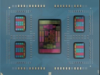
![]()
The main thing to contemplate is that the memory hierarchy will be getting richer and deeper, and memories of various kinds will be pulled closer to the CPU complex in a server. This will presumably have dramatic impacts on the utilization of CPUs and how much work can be pushed through the system at a given price. Forgetting that last part – at a given price – is sometimes hard in the excitement around new technologies. But weighing those different memory technologies against each other – in a raw sense as well as when running real applications – and taking into account their price/performance will be a real challenge for IT organizations. So will be writing applications that know the difference between and can take advantage of the wide variety of volatile and non-volatile memories that will be available in future servers. That’s why we will be talking to the experts about the possibilities.
PCI Express And Network I/O
With the advent of non-volatile memory that comes in a DRAM form factor, hooking a reasonable slice of persistent memory into a server with very fast access is going to be a fairly simple affair. The rest of the I/O devices crammed into or hanging off the server will have to get to the CPU through PCI-Express interfaces, proprietary interfaces like IBM’s Coherent Accelerator Processor Interface (CAPI) for Power8 chips or like Nvidia’s NVLink with its Pascal Tesla cards, or Ethernet or InfiniBand network interfaces.
Every new generation of processor, storage, and networking has its challenges, and PCI-Express has certainly had those and, in fact, that is why IBM’s CAPI and NVidia’s NVLink were invented. PCI-Express 1.0 was launched in 2003 with devices able to push data at 2 Gb/sec (250 MB/sec) per lane each way, and in 2007 that was bumped up with PCI-Express 2.0 to 4 Gb/sec lanes (500 MB/sec). With PCI-Express 3.0 in 2010, the speed was doubled up again, with lanes running at 8 Gb/sec (1 GB/sec). Development on the PCI-Express 4.0 spec started in earnest in 2011, with another doubling up of bandwidth to 16 Gb/sec per lane (which is 2 GB/sec), and many had hoped to see it come to market in 2016, but it is looking more like it will take until 2017 or more before the first products come to market. The Skylake Xeons, tellingly, will sport PCI-Express 3.0 controllers and peripherals when they come out, probably in late 2017.
The question we have is whether the CPU memory bus and PCI-Express 3.0 peripheral bus will be up to the extra demands that will be put in them by processors with more cores and cache and all of those myriad memory and storage devices. It will be interesting to see how the system architects build their iron.
Related Items
Future Systems: Can Exascale Revive AMD?
Future Systems: Intel Ponders Breaking Up The CPU
Future Systems: Pitting Fewer Fat Nodes Against Many Skinny Ones
Future Systems: Intel Fellow Conjures The Perfect Exascale Machine
Future Systems: How HP Will Adapt The Machine To HPC


Injecting Machine Learning And Bayesian Optimization Into HPC
No matter what kind of traditional HPC simulation and modeling system you have, no matter what kind of fancy new machine learning AI system you have, IBM has an appliance that it wants to sell you to help make these systems work better – and work better together if you …
Big Blue Turns In A Solid Quarter For Systems
By all accounts, Big Blue had a pretty good quarter ending in June, with sales of its System z16 mainframes skyrocketing upwards as they do every couple of years at the beginning of a new cycle and sales of its high-end Power10 machines also getting some traction. If everything goes …
Debunking Datacenter Compute Myths, Part One
There has always been a certain amount of fear, uncertainty, and doubt that IT vendors sow as they try to protect their positions in markets that they participate in. But there is also a lot of straight-up misunderstanding among those vendors as well as the people who work at the …
I think the TOFU 2 interconnect is very interesting and worth a mention too.
As well as Knights Hills allegedly having the first silicon photonics from Intel.