

We spend a lot of time in the upper stratospheres of computing among the hyperscale and HPC crowds here at The Next Platform, and the consistent theme across these two similar but often very different customers bases is that we need a new system architecture that provides better performance at a lower cost and in a lower thermal envelope and an expanded memory hierarchy that can help with those goals.
We don’t know what the hyperscalers are up to when it comes to future systems designs – they keep these largely under wraps and rarely give us a peek into their systems. But we are getting some insight into what the HPC community is doing as it tries to come up with systems that combine various compute, memory, and I/O technologies that can deliver exascale performance and data storage. As has happened many times in the past, we believe that the ideas and technologies behind HPC system designs will eventually cascade down to large enterprises, perhaps with tweaks here and there to account for differences in workloads and capacity needs. Some technologies simply do not scale down well, or do not fit into the very regimented and inertial environment of the corporate datacenter.
The point is, by looking at possible compute, memory, and I/O components of HPC systems designed to scale beyond petascale into exascale territory – systems that the Obama Administration embraced with its National Strategic Computing Initiative announced this week – we can get a read on what the future might look like and start working towards that.
AMD has had its share of woes in the system business in recent years and recently hit reset on its server business, shutting down its SeaMicro microserver business back in April and mothballing its “SkyBridge” effort to make its Opteron X86 and ARM processors socket compatible. Under new CEO Lisa Su, AMD has hired a slew of server experts, notably Forrest Norrod, who ran Dell’s custom server business as well as its overall PowerEdge server business and who is now general manager of AMD’s Enterprise, Embedded, and Semi-Custom Business Group. That embedded group, which is making processors and graphics units for Microsoft and Sony game consoles, is the bright spot at AMD these days as its server business has dwindled and the PC market continues to decline. And AMD wants to take the expertise that it still has in systems and has built up with hybrid CPU-GPU computing and bring that into the datacenter. While the company’s roadmaps are a bit thin – and intentionally so because Norrod does not want to tip AMD’s hand about what it has planned for the future – the chip maker says it is steadfastly committed to getting back into the datacenter and it will be using HPC as a lever to do this.
AMD divulged back in May that it is working on a new X86 core design, code-named “Zen,” which will have some form of simultaneous multithreading (SMT) like Intel Xeon, IBM Power, and Oracle and Fujitsu Sparc processors have. SMT adds virtual threads to a core so it can look like two, four, or eight virtual processors to the operating system and multiplex instruction processing across those threads to boost calculation throughput. AMD has never added SMT to its chips before. AMD is also promising that the next-generation of Opterons will have “disruptive memory bandwidth” and “high native I/O capacity” and that the Zen cores will deliver 40 percent more instructions per cycle (IPC) than the “Excavator” cores used in its current CPU-GPU hybrids, which it calls APUs, short for accelerated processing units.
Interestingly, and relevant for the future systems conversation, AMD revealed that it was working on a CPU-GPU hybrid that would have “multi-teraflops” of computing power. Since early this year, rumors have been circulating about a Zen-based chip that has 16 cores with a total of 32 threads, with 512 KB of L2 cache per core and 32 MB of L3 cache shared across those cores. This rumored Zen chip, which AMD has not confirmed the existence of, also has a “Greenland” GPU with an unknown number of graphics cores plus 16 GB of high bandwidth memory (HBM) on the chip package that sports 512 GB/sec of bandwidth, plus four DDR4 memory controllers to access additional memory and 64 lanes of PCI-Express 3.0 I/O to link out to other peripherals. It is not clear if it has integrated networking, but variants certainly could.
As it turns out, this is exactly the kind of motor that AMD has been talking about as part of its system designs under the Fast Forward and Fast Forward 2 contracts with the US Department of Energy. The Fast Forward work gives AMD tens of millions of dollars to do basic research into how to build a system node based on a hybrid compute element, which it has been working on since late 2012 when the first awards went out. AMD is pretty secretive about the results of the study, but some information about the initial Fast Forward effort was made public and researchers at AMD have also published a paper in the July/August issue of IEEE Xplore that reveals some of the system design concepts they are developing. Here is what the initial Fast Forward concept looked like:
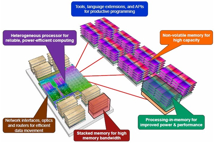
You will notice a few things to start. First, the Fast Forward concept stacks up memory close to the CPU-GPU hybrid compute to get the high bandwidth that applications require and cannot get with GPUs linked to CPUs over PCI-Express peripheral buses. The hybrid compute chip will have a single virtual address space, thanks to AMD’s Heterogeneous Systems Architecture (HAS) electronics, which by the way will be extended to work across discrete Opteron CPUs and AMD GPUs and is not limited to on-die setups. HSA applies equally well to X86 and ARM cores, and the pointer-based structures will allow for data to be shared between CPUs and GPUs where it sits in the memory. No more copying between devices. AMD is working to make HSA compatible with FORTRAN, C, C++, C++ AMP, Java, OpenCL, OpenMP compilers and programming models, and says that while it is focusing on GPUs at the moment, it could extend HSA to other kinds of accelerators (such as FPGAs) or to other devices (such as network interface cards).
This on-package memory architecture that AMD is describing is similar to that which Intel is employing with its impending “Knights Landing” Xeon Phi massively parallel processors, you will recall. Knights Landing has 16 GB of HBM near memory on the package with more than 400 GB/sec of bandwidth and up to 384 GB of DDR4 far memory linked to the 72 cores on the die with up to 90 GB/sec of bandwidth. The compute package on this concept compute node also has network interfaces, optics, and routers integrated so data movement between nodes is efficient and fast.
The other neat bit in the AMD future system design is the introduction of a non-volatile memory storage layer that is off the core compute package that has its own processing so data can be preprocessed where it is sitting on that non-volatile memory.
In the IEEE Xplore paper, AMD’s researchers laid out the problem a little more clearly. The problem, they explained, is that to build an exascale machine will require as many as 100,000 server nodes, and each one has to deliver around 10 teraflops of double precision floating point performance as well as enough integer performance to be useful on other kinds of workloads besides simulation and modeling. (The convergence of big simulation and big data is unavoidable.) All of this has to be done in a power envelope on the order of 20 megawatts or less if it can be done, but this is by far not the only issue even if it is the most overbearing of the constraints imposed on exascale systems. (We would say cost is the second issue, but this also relates to power consumption, ultimately.)
The architecture of what AMD is now calling an exascale heterogeneous processor, or EHP, has not changed all that much in the past year. Here is the latest block diagram from AMD:

In the conceptual processor above, you can see the GPU is front and center, with 32 CPU cores wrapped around it. There are eight banks of 3D stacked DRAM memory to keep this compute element fed with data; presumably the cores have L1 and L2 caches, and possibly shared L3 caches, too. AMD is not saying. The off-chip NVRAM memory could be any number of technologies, and it could even be the new 3D XPoint memory that rival Intel and Micron Technology announced this week. (There are a number of different memory technologies that can fulfill this secondary storage role, and we outlined many of them, thanks to Micron CTO Dean Klein, here.) What the non-volatile memory technology is will depend on the market a few years hence, but the issues that AMD lays out are the real problem.
The Department of Energy wants an exascale-class system to have at least 1 TB of memory and support up to 4 TB/sec of aggregate memory bandwidth per node. Current CPU-only systems are off by a factor of 100X and that rumored AMD Zen-based hybrid and the Intel Knights Landing processor will be off by a factor of eight or so. Even the conceptual design shown by AMD above, with eight stacks of HBM on the package, will top out at 1 TB/sec of bandwidth. Monkeying around with signal rates, bus widths, and channel counts, AMD says, could get it up to the 4 TB/sec range in the exascale timeframe – call it 2020 to 2022 or so – but then the capacity gap will still be wide if the device can only support 128 GB of near memory as AMD expects. The memory capacity gap is actually harder to close than the memory bandwidth gap, which was surprising to us until we read this AMD paper. For server nodes that require even more capacity, AMD says the idea will be to plug in a tertiary level of NVM – likely using another technology such as NAND flash or memristors should they ever come to market.
If all of this memory innovation can come to pass, the energy bill is still going to be crushing for this memory.
“Even with aggressive assumptions about memory and interface technology improvements reducing total DRAM access energy from approximately 60 to 80 picojoules per bit for DDR3 to 2 picojoules per bit,” the AMD researchers write, “we project that sustaining 4 TB/sec could consume more than half of the entire exascale system’s power budget on memory accesses alone. Processing in memory (PIM) implemented via 3D die stacking allows some computation to be moved close to the data, enabling high memory bandwidth with reduced energy consumption per access.”
Not surprisingly, AMD is suggesting that for HPC workloads, the perfect processor for chewing on data out in those PIM modules is a GPU. And suffice it to say that all of these different memory layers could make it very difficult to program. Obviously, HSA abstraction would be useful if it could be spread across the storage domains as well as compute, but it is not clear how far HSA can be pushed.
This is all very interesting in theory, but it is not at all clear how AMD will capitalize on this research and infuse it into products that HPC and hyperscale customers will buy. But that is clearly the goal, and if AMD can work with memory and interconnect partners to flesh out this exascale architecture – much as IBM has done with Nvidia and Mellanox Technology with the OpenPower Foundation – it has a chance to carve itself out a piece of the business.


China Has Already Reached Exascale – On Two Separate Systems
More analysis “Why Did China Keep Its Exascale Supercomputers Quiet?“ Native CPU and accelerator architectures that have been in play on China’s previous large systems have been stepped up to make China first to exascale on two fronts. The National Supercomputing Center in Wuxi is set to unveil some striking …
AMD Finishes Out The Zen 4 Server CPUs With Edgy “Siena”
Different workloads need different mixes of price, performance, thermals, and longevity in the field out there on the edge and in the datacenter, and that is why server CPU makers for years have had a mix of processors that deliver on these vectors that are different from each other. What …

With Vista, TACC Now Has Three Paths To Its Future Horizon Supercomputer
The national supercomputing centers in the United States, Europe, and China are not only rich enough to build very powerful machines, but they are rich enough, thanks to their national governments, to underwrite and support multiple and somewhat incompatible architectures to hedge their bets and mitigate their risk. In the …
Since early this year, rumors have been circulating about a Zen-based chip that has 16 Zeon cores with a total of 32 threads, with 512 MB of L2 cache per core and 32 MB of L3 cache shared across those cores.
I believe you meant 512KB of L2 cache per core.
Yup. Thanks. My dyslexia was running high.
I am not too optimistic that we’re going to see AMD back in the game unless they pull off a miracle with Zen looking at the track record and all the trouble and shuffling that has happened in the last 5 years of AMD it doesn’t feel very likely. They are quickly running out of money which makes it difficult to spend on significant R&R required to stay in the game. I don’t see a coherent strategy at AMD either first they buy SeaMicro an expert and at its time a leader in low power fabric compute nodes and then ditch it a few years later.
Really the Xeon PI with HBM, and the AMD APU with DRAM, and AMD is Currently using HBM, which it and its partner engineered. The Xeon Pi’s does not use HBM, and to date AMD is the only one using HBM in a product. So what is the number of FP units on the AMD GPU in the diagram. I think you mean HMC on the Xeon, and the article needs to be corrected. I’d like to see more information on the AMD APU, and that includes the possibility that the GPU will have a little more FP resources on its Die than even the latest Xeon Pi can provide. That and any information on AMD’s patent filing for an FPGA integrated on the HBM die stack between the bottom logic chip and memory dies above. Intel’s 72 cores are still not enough compared to the thousands of GPU cores on the AMD APU. With all the computing workloads shifted to the GPU, the old IPC argument for CPU cores as a defining feature is not going to hold as much weight as it has in the past. AMD’s APUs are becoming more integrated with the GPU, at some point in time there will be CPU cores directly dispatching FP work to the GPU as HSA progresses. I do not see Intel getting the work done without some GPU acceleration on its products, and AMD is the only one that is tightly integrating GPUs with CPU its cores, and already has the GPU accelerators in house. Zen’s IPC performance need only get close to Intel’s and the GPU side of the equation will deliver the needed computational performance. How Intel can remain using only x86 cores, and hoping to compete with the Power based systems and Nvidia accelerators, and AMD’s tightly integrated HPC APUs. More interesting is the possibility that AMD could do a little more with its K12 custom ARM cores and go the SMT, route with a Power8/Power style wide rank of execution pipelines and more than 6 processor threads per core, or even that AMD itself could get an OpenPower license and engineer a power based APU, for say Facebook or another custom server client. AMD does have some success in the custom services area. SeaMicro may be shuttered along with projest sky bridge, but SeaMicro’s IP is still of value in future SKUs for third party server OEMs.
XEON Phi are general purpose cores, GPUs are very SIMD. They’re different beasts.