
The best minds in networking spent the better part of two decades wrenching the control planes of switches and routers out of network devices and putting them into external controllers. We called this software-defined networking, or SDN, and it gave network operating centers a holistic view of the network and made that externalized control plane programmable – meaning, responsive to current and, increasingly, future traffic patterns to help it flow better and operate efficiently.
A similar “software-defined” battle has been going on inside of switches and routers themselves at the data plane, which controls how data moves inside of, is processed by, and increasingly augmented by packet processing engines that are themselves programmable like CPUs and GPUs.
Well, not exactly like CPUs and GPUs, because networking – by which we mean understanding Ethernet packets of various shapes and sizes and getting them from endpoint A to endpoint B in a network that might have hundreds of thousands to millions of endpoints so that computation and storage can occur – is a very different animal from compute and storage.
Switch and router ASICs are a very precise kind of computation, and general purpose compute engines like CPUs and GPUs are terrible at doing packet shifting work. We all learned this in the first wave of SDN products. (Remember when Intel was eagerly talking about replacing switches with Xeon processors?)
But just because an X86 chip make a terrible switching device does not mean that switch and router ASICs should not be more malleable than they are. And just because we have merchant silicon from several suppliers and Linux-based network operating systems (many of them open sourced as well) does not mean that switch builders and their customers have access to low-level features in those ASICs or that they are programmable to the degree and using the languages that such customers want. (Meaning, the hyperscalers, cloud builders, telcos, and other service providers as well as hotshot financial services firms and maybe a few HPC centers, too.)
We were very excited on your behalf when Barefoot Networks dropped out of stealth mode in June 2016 with its “Tofino” programmable switches and a commercialized variant of the P4 programming language created for networking. Barefoot Networks made every one of the merchant silicon vendors open up their SDKs a little bit and give customers more control if they wanted it, which was a good thing. But, sadly, Intel bought Barefoot Networks in June 2019 for an undiclosed sum to get back into Ethernet switching – it had bought Fulcrum Microsystems in July 2011 and ultimately did not do much with it – and after the company’s datacenter business went up on the rocks a few years later, Intel shut down the Barefoot Ethernet switch business in January 2023 without really doing much with it.
This leaves the field pretty much wide open for big disruption as far as Xsight Labs, a networking startup founded in 2017 and that dropped out of stealth in 2020 (sort of), is concerned.
Open For Business
To be fair, Broadcom has been increasing the programmability of its Trident, Tomahawk, and Jericho lines of switche ASICs over the past decade, and has open sourced its own switch programming language, called NPL. After this story ran, Broadcom reminded us that it announced the Trident 5-X12 for next-generation top of rackers back in November 2023 and that ASIC, says Broadcom, has a higher level of programmability than the Tofino chips offered. The state of the art has moved ahead perhaps more than anyone realizes when it comes to switch programmability.
Marvell has some level of programmability in its switch ASICs, but, as far as we know, not to the level that Barefoot Networks and Xsight Labs aspire to in their mainstream products.
The Spectrum 3 and Spectrum 4 ASICs for Ethernet switches from Nvidia (formerly Mellanox Technologies) are programmable at the data plane level, and so are the Silicon One ASICs for switches and routers from Cisco Systems (but not all of them have this functionality fully activated). Ditto for Broadcom’s Trident, as mentioned above.
You can open a whole can of worms about whose switch ASICs are more programmable, and where in the chip — in the parser, in the ingress and egress of the device, in the other components — and frankly, maybe we should revist that can of worms at some point.
Pensando (now part of AMD) and Fungible (now part of Microsoft) had programmable DPUs, but did not make programmable switch chips, or indeed any switch ASICs at all. Perhaps they should have. And perhaps Cisco should have made its own DPU, while we are thinking about it. Nvidia has InfiniBand and Ethernet switches and a set of SmartNICs (ConnectX) and DPUs (BlueField) that they share.
It is arguable, however, that Xsight Labs is trying to push programmability to the extreme, eventually allowing customers to use P4, Python, C/C++, Rust, Go, or what have you (maybe even NPL) to hack the data plane inside switches using its X1 and now X2 ASICs. It might be a combination of many languages in the end, which of course is what programmers love because they get to indulge their preferences and avoid their prejudices.
What programmers might also love is an open instruction set architecture, by which we mean the specs are all fully documented and whoever created the architecture is not demanding licensing and royalty fees if you use it. And starting this week, Xsight Labs is opening up its network chip ISA to any and all so they can create applications that run atop switches using its ASICs and DPUs that it makes or that others could make using its E1 DPU chip. If you want to clone the company’s switch or DPU chips, or create a variant, have at it.
There are very few open ISAs out there in the CPU world, and none in the network ASIC and NPU world as far as we know until now. Let’s think about the CPUs that have open ISAs for a second.
RISC-V is not only open, but some contributors go all the way and give away the RTL describing the chips that are made. RISC-V might be the future, but that future might be largely a post-economic one.
Arm creates an architecture that has become ubiquitous, but you have to license it and you have to pay royalties.
Intel created the X86 architecture, and AMD arguably improved it with all kinds of innovations. In theory, either Intel or AMD could license the X86 ISA, but heaven only knows what outrageous price it would charge. But because they wanted ubiquity of software, the X86 ISA is published, and that has indeed been helpful in allowing the X86 architecture to take over the datacenter for maybe a decade and a half.
Sun Microsystems opened up the Sparc ISA way back in 2006, a few years before Oracle ate it the company, and IBM opened up the Power ISA starting with Power8 in 2019 and continued up through Power9 and Power10. A decade ago, MIPS Technologies (the CPU spinout of the original Silicon Graphics) opened up its ISA to try to save it; now MIPS, after many permutations as part of Imagination Engineering and Wave Computing, is peddling RISC-V cores.
It is hard to say how opening up the Xisa might help Xsight Labs at the front end of a business because that generally has not happened with CPUs. Opening an ISA has been a kind of penultimate-gasp move, RISC-V and now the Xisa used in the X1 and X2 switch ASICs and the E1 DPU, where it is being done very early in the cycle. An open ISA is a good thing, but we don’t know how critical it will turn out to be. It all depends on what people do with it, really.
X Is A Function Of Why
Many of us have been waiting to see how Xsight Labs would shake things up in datacenter networking, and now we are starting to get a feel for it.
In part, that expectation for big change comes from the fact that Avigdor Willenz is the company’s founding investor. Willenz founded Galileo Technology, a maker of Ethernet switch ASICs that sold to Marvell in 2001 for $2.7 billion, and that wealth has been spread around. Willenz invested in Annapurna Labs, which sold to Amazon Web Services in 2015 for $350 million and which has created its Nitro DPUs, Graviton CPUs, and Trainium and Inferentia AI engines. He was president (now chairman) and first investor in distributed flash block storage maker Lightbits Labs. Willenz was a co-founder of AI chip maker Habana Labs, which sold to Intel in 2019 for $2 billion and is the foundation of its Gaudi compute engine line.
The other reason to expect big changes is that Guy Koren, Erez Sheizaf, and Gal Malach, who all worked at EZchip, a DPU maker that was eaten by Mellanox in 2016, leading to the BlueField SmartNICs that are now at the heart of Nvidia’s DPU strategy, founded Xsight Labs. They know networking and networking processing. The company has nearly 200 employees and more than 40 contractors, and which includes experts from Cisco, Mellanox, Broadcom, Intel, and others. The company is co-headquartered in Tel Aviv and San Jose, with development labs in Billerica, Massachusetts and Raleigh, North Carolina.
Xsight Labs has raised $281 million in four rounds of funding, and counts Intel, AMD, Microsoft, Valor Equity Partners, Battery Venture, Michael Dell, Accton Technology, and Fidelity as investors beside Willenz.
As we have said previously, we are amazed that Amazon has not bought Xsight Labs already, or that AMD, which also has networking aspirations, has not, too. With a valuation of around $1.1 billion after its $116 million Series D funding round in the spring of 2023, it would presumably not be too expensive these days for either company to do so. Perhaps it will be cheaper for AWS to be a customer and for AMD to recommend Xsight Labs resellers. . . .
X Marks The Spot
Let’s drill down into the tech a little bit, which will reveal why an open ISA could be very important for driving adoption of the X1, X2, and future X3 silicon from Xsight Labs.
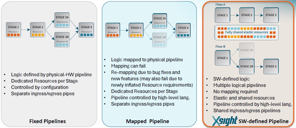
First, we need to compare and contrast the level of programming in the switch ASICs. As the chart above showed, switch ASICs from days gone by had fixed pipelines in their packet processors, which are generally wrapped by the SerDes that provide signaling to the outside world. Over time, more and more programmability has been added to switch (and router) ASICs, basically because we have been spoiled by the absolute programmability of CPUs.
“Our vision is software defined – everything truly software defined and truly open,” Gal Malach, who is chief technical officer at Xsight Labs, tells The Next Platform. “A lot of the focus now is on the X2 and its full program ability, which is unlike anything that else that’s out there.”
Malach laid this chart on us to differentiate, and it is something that we might have expected to see out of Barefoot Networks with Tofino:
And then he offered this explanation:
“With the switch ASICs with fixed pipelines, the logical pipeline is defined by the hardware pipeline, and you don’t have a lot of flexibility. You do have some configuration, which, you know, this is something that the silicon vendors open for you. If it’s not there, it’s not there. In most of the cases, the resources are attached to specific stage. So again, you don’t have any flexibility to use one resource at a different stage. In most of the cases, you have a separate ingress and egress pipe, which means you can deliver some metadata and information from one pipe to the other.”
“In the middle, I will call this the map pipeline, which is like a Tofino use case, others will say that maybe Cisco Silicon One falls into this category, too. Here, you still have a pipeline. It’s a superset of a pipeline with many, many features and many, many resources. But again, the resources are attached to their stages within the pipeline. And now, using P4 as an example, you can actually define your logical pipeline and there is a compilation process. They take in the logical pipeline and map it over the physical pipeline, which works great. It gives you much better flexibility and a richer feature set. But then, when you are trying to fix a bug in the P4 code, and you edit few more lines, then the mapping is no longer valid, and sometimes you need to refactor the entire P4 program because you lack of resources where you need them. Sometimes you just don’t have enough resources to do some pipeline folding, which means that we’re taking two pipelines connecting them together, which means that latency will be double, power will be double for that specific application.”
“We are offering a totally different approach. We are not implementing your pipeline. We don’t have a pipeline. You actually use the software to define your logical pipeline. So there are no constraints here because there is no mapping. This is a bit like X86 processing in that you have an instruction set and you have a memory, and you can use the resources the best way that fits your application. So all the resources are fully shared and elastic. So with Xisa if you want more counters, go ahead, use the memory for counters. If you want a larger L3 table, go ahead. If you don’t need L2 don’t define the table at all. You control all of the resources because that’s the best way to serve the application. Everything is software defined – the tables, the counters, the entries, and obviously the program, which is again based on dedicated instruction set, which we have opened.”
The X-Switch chip hardware has two main stages to create a programmable forwarding engine, or PFE:
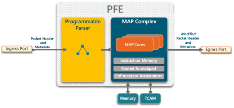
The programmable parser stage does just what you think it does: It reads metadata and slices up the packet headers of an Ethernet packet. This of it as a kind of DPU in front of a CPU to preprocess the packet. The Match-Action Processor, or MAP, is really a collection of tens of packet processing cores with instruction memory, scratchpad memory, and hardware accelerators, and each MAP core handles one packet from ingress to egress. The MAP complexes are integrated into a matrix of data path units (confusingly also called DPUs), which are surrounded by interface units, or IFUs, that contain Ethernet MACs and SerDes blocks for signaling. It is a massively parallel, reconfigurable, packet processing engine. Like if a programmable dataflow engine had a lovechild with a switch ASIC.
The upshot of this programmability is that the user, not the switch vendor, gets to turn the knobs on resources to decide if they want to have a port to port hop latency of 700 nanoseconds or 400 nanoseconds depending on the nature of the overall application and its latency needs. If you map more resources to certain kinds of packets and run it in parallel, you cut the latency. It’s that simple. Like programming a GPU with lots of CUDA cores, perhaps.
Here is the other neat thing. Xsight Labs is not all that worried about what the Ultra Ethernet Consortium spec will do. Because everything – and we mean everything – that it does on the X1 and X2 switch is done in software, not hardware.
“We taped out the X2 even before the first version of the Ultra Ethernet spec will be released,” says Malach with a laugh, “because whatever is needed there – like back to sender, packet trimming, packet spraying, whatever – everything we do is software defined.”
It starts with congestion-aware routing, which includes user-defined metrics (rate, latency, queue fill, or a mix), congestion signaling at the data plane using ECN, CSIG tag, or whatever a hyperscaler or cloud builder already has cooked up, and several kinds of load balancing, including flowlet-based in order or packet spraying out of order techniques that rely on DPUs at the end points to get the packets all back into order.
The X2 ASIC also has a 64 MB shared memory buffer that helps with network incast tolerance in a single switch and uses a mix of congestion telemetry and BCN messaging to keep the top of rack and spine switches from swamping a switch with elephant flows.
And for the record, a lot of what will be in the UEC spec has already been added to the X2 software stack. That includes packet trimming (cutting up big packets into smaller ones to get around traffic jams, akin to converting a tractor trailer into a fleet of motorcycles on a highway), back to sender congestion signaling, and adaptive packet spraying.
So where is Xsight Labs at with its hardware? The X1 switch ASIC was quietly unveiled in December 2020, and it came in three versions, one with 25.6 Tb/sec of aggregate bandwidth and two with 12.8 Tb/sec of aggregate bandwidth. The top-end part had 256 SerDes running at 100 Gb/sec, the middle part had 128 SerDes running at 100 Gb/sec and the entry one had 256 SerDes running at 50 Gb/sec. (We would have called that latter one the X0 to avoid confusion.) That top-end X1 could deliver 256 ports running at 100 Gb/sec, 128 ports at 200 Gb/sec, or 64 ports at 400 Gb/sec.
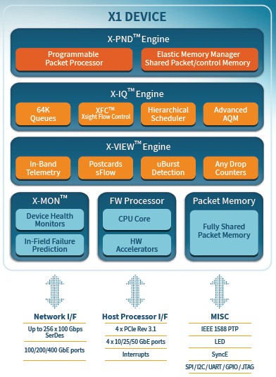
The 12.8 Tb/sec version of the chip did half the number of ports at the same speed. We presume both were etched in 7 nanometer processes from Taiwan Semiconductor Manufacturing Co. These chips were used mostly as a development platform, and did not go into volume production as far as we know.
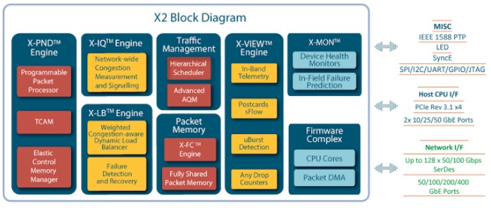
Malach says that the X2 device uses 5 nanometer processes from TSMC, and has a 40 percent reduction in power consumption compared to the most-like X1 device. Port hops range from 700 nanoseconds to 450 nanoseconds as well. The first X2 chip delivers 12.8 Tb/sec of aggregate bandwidth and is aimed at top of rack use cases with 100 Gb/sec ports down to servers and 800 Gb/sec ports up to leaf switches.
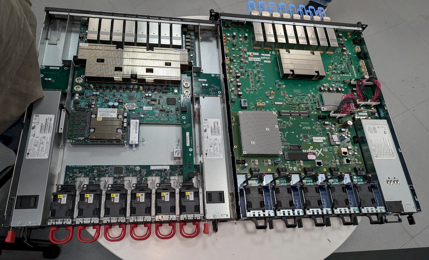
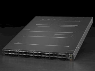
The X2 chip started sampling in July 2024, and will be shipping with switch makers starting in April with whitebox switch maker Accton getting first in line. That is the Accton X2 switch on the left in the picture below, and the Xsight Labs development platform using the X2 on the right:
Xsight Labs plans to deliver versions of the X2 running at 6.4 Tb/sec, 8.0 Tb/sec, and 9.6 Tb/sec to provide four 800 Gb/sec uplinks and 32 200 Gb/sec and 48 100 Gb/sec downlinks, respectively.
And as you can see from the chart below, showing 400 Gb/sec end-to-end connectivity across TOR, leaf, and spine layers in the network, there is a plan to scale up to 1042.4 Tb/sec X2 devices:
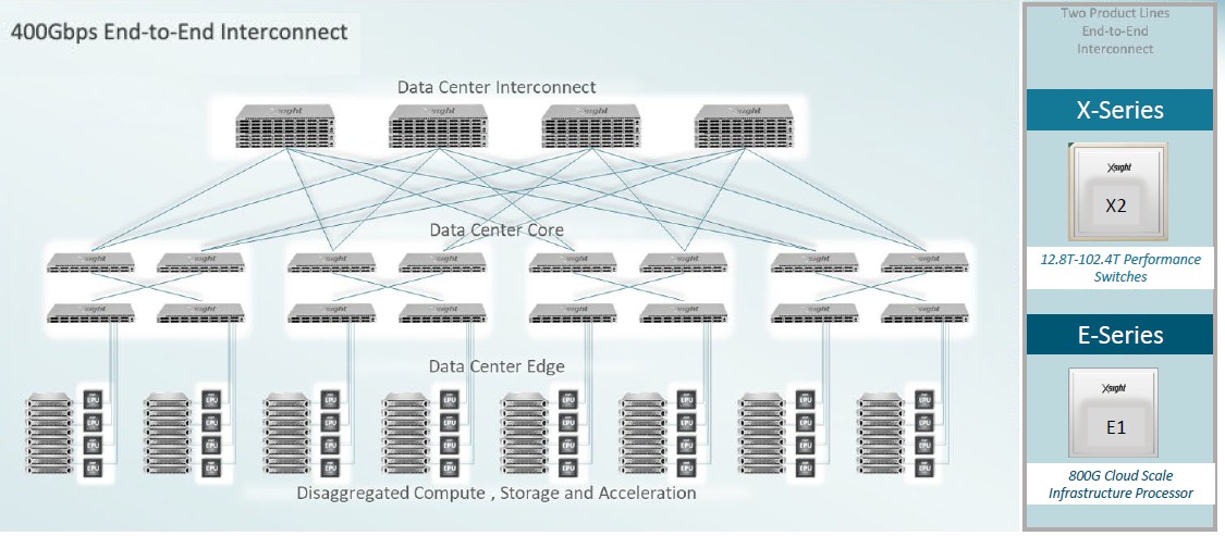
Presumably there are 25.6 Tb/sec and 51.2 Tb/sec devices as stepping stones up to that higher aggregate bandwidth, and we presume that the more capacious devices have a chiplet design breaking the SerDes from the packet engines, and perhaps modularizing the packet engines, too, and lashing them all together with chip-to-chip interconnects.
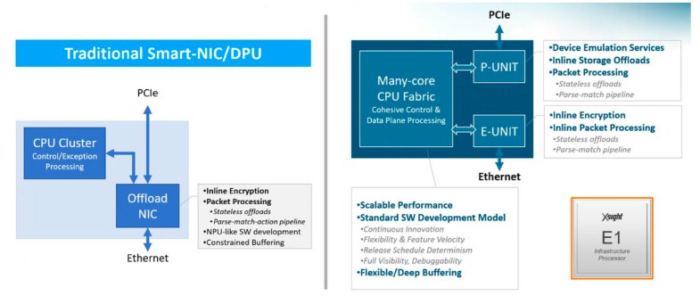
That brings us to the Xsight Labs DPU endpoint, the E1. With many DPUs, says Malach, a NIC with a certain amount of brains is augmented with some CPU cores to do auxiliary work out of the data path. With the E1 DPU, Xsight Labs is putting 64 Arm Neoverse N2 cores right in the data path.
The E1 chip is etched in 5 nanometer processes from TSMC, like the X2 switch chip. Here’s the block diagram for the E1:
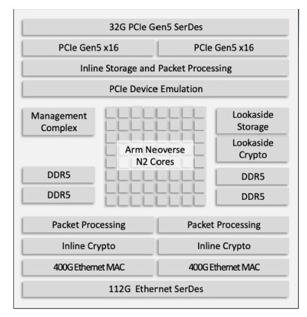
With all 64 cores activated, the E1 DPU will run about 90 watts and with 32 MB of L2 cache and four DDR5 memory channels. A version with half the cores and memory will run about 65 watts.
Think of it as your own personal Nitro card. . . .
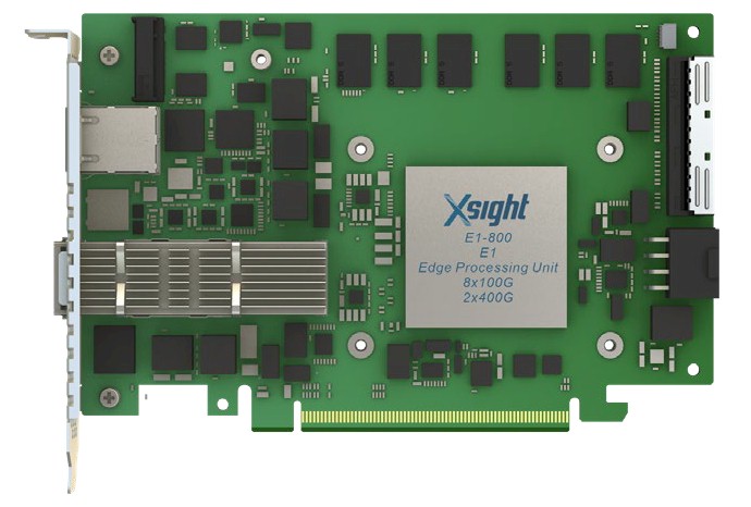
The E1 can implement two 400 Gb/sec ports, four 200 Gb/sec ports or eight 100 Gb/sec ports, and it can run Debian and Ubuntu Linux and the Microsoft’s SONiC network operating system unmodified. Which makes sense because it is really just a baby Arm server that has some Ethernet ports and network accelerators on it.

The Eternal Battle Between InfiniBand And Ethernet In HPC
It is always good to have options when it comes to optimizing systems because not all software behaves the same way and not all institutions have the same budgets to try to run their simulations and models on HPC clusters. For this reason, we have seen a variety of interconnects …
Why Would HPE Buy Juniper Networks?
It looks like Hewlett Packard Enterprise might be having a datacenter networking revival. The word on the street, as reported by the Wall Street Journal, is that HPE is getting ready to shell out $14 billion to acquire Juniper Networks, the company that played the gadfly for Internet routing and …
Nvidia Hints At Upcoming AI-Focused Spectrum-4 Ethernet
It is no surprise at all that Nvidia’s datacenter business is making money hang over fist right now as generative AI makes machine learning a household word and is giving us something akin to a Dot Com Boom in the glass houses of the world. It is also no surprise …
Be the first to comment