

When it comes to deep learning chip startups, hype moves fast but crossing the finish line to real production silicon takes an incredibly long time.
There are several incumbents on the custom hardware side aiming for the AI training and inference market but outside of Google’s TPU, there are very few functioning inside datacenters. From the forthcoming Nervana chips (now expected in 2019) to startups like Graphcore, Cerebras (which just ducked back into stealth mode), among several others, the pressure is on to create hardware that reflects the latest framework and algorithmic developments that so far seem to run quite well on widely available GPUs with all the requisite porting and software work handled thanks to big library and tooling investments from Nvidia over the last few years.
In other words, it is going to be damn tough to beat Nvidia, especially this late in the game, but for one of the better known deep learning chip startups, Wave Computing, there is more going on in the outfield than we might readily see. This is why the company has invested in tech that might seem a bit left field—that is, until we look at how the AI hardware game of the future might play out. On top of that, they are winding up with their first pitch into real systems and customers, beginning with a four-DPU box for early customers based on silicon that arrived in December 2017.
We learned that Wave will be announcing that they are acquiring MIPS Technologies, which has specialized in RISC IP and core licensing with over 350 patents that fall into the deep learning chip startup’s hands. One could posit a guess that Wave was being defensive (or offensive, depending on how one looks at it) by moving fast to protect itself against future chips from those other incumbents, but this is not so, according to Lee Flanagin, SVP and chief business officer at Wave. He says that while the addition of MIPS patents adds to their overall value, the acquisition is all about the market—one that gets even more valuable closer to the edge.
“We have a bolstered patent portfolio after this for sure, but the opportunities around this have nothing to do with any offensive or defensive move for patents. It’s a market play—and this is where the technology supports the market strategy,” Flanagin says.
Financial details of the deal have not been disclosed but Flanagin says it leaves Wave, which has taken $117 million funding, ending most recently in Series D that included (now confirmed) Samsung, in net positive territory. “This is immediately accretive and cash flow positive to Wave. The timing makes sense; now that we have the foundation it is time to take our first real steps.”
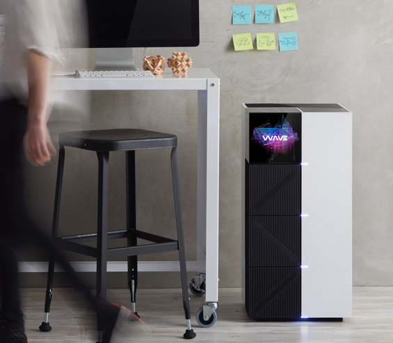 That foundation he speaks of is the arrival of real silicon, which will be presented to Wave’s first customers in the form of a workstation appliance in the next couple of weeks. This is an interesting development for the ecosystem of AI chip startups because it marks a concrete product—something that is sorely lacking.
This initial workstation product can be plugged directly into the wall and is designed to live outside the datacenter for training and inference experiments or limited scale production workloads. Wave expects this will be used for testing and hyperparameter tuning as it allows packaging up of models into containers for deployment elsewhere. In essence, it is a TensorFlow box with two single gigabit Ethernet and two 10GbE ports as well as 8 TB of storage.
As you might recall from the first deep dive we were given over a year ago into the Wave Computing architecture, there are over 16,000 processing elements on each chip (TSMC 16nm).
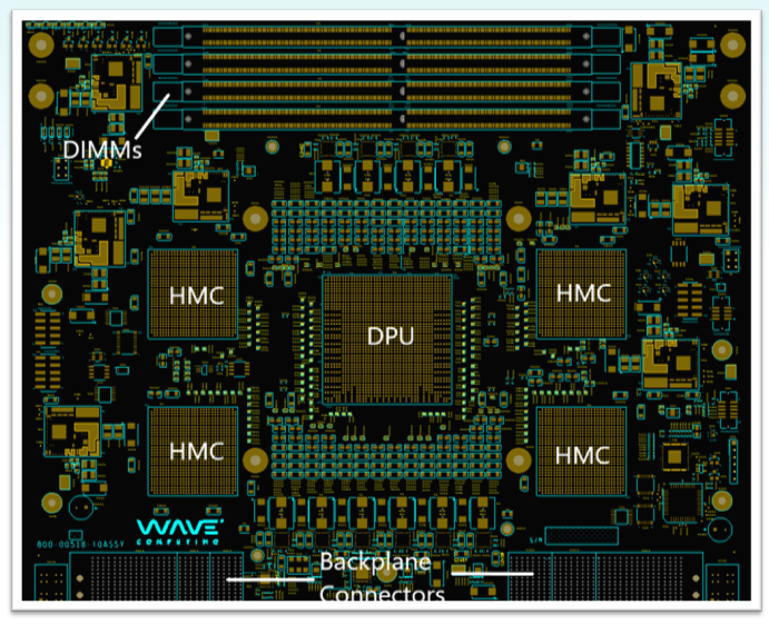 Four of these chips plug into the backplane, which is fronted by a single board computer with hybrid memory cubes (HMC) serving as connector and communicator versus switches. Recall that with Micron’s chaining tech on HMC devices, it is possible to get direct point to point communication. As we explain in the original architecture article, all communications pipelined and delivered as dataflow graphs across the hybrid memory cubes. Again, if one wants to argue that memory is the next platform for some deep learning workloads, this is a good representation.
Even though plenty of work will go on and off the chips and boards, the latency hit is expected to be no worse than with NVlink and NVswitch on a DGX-1—something we will see play out when the first benchmarks of Wave’s hardware come out (an MLPerf benchmark story we are following for future publication). Flanagin says the first customers making use of the system are using time series data—a potential hint that this is a financial shop, but that is just our own speculation since we know these users to be first in line to sample new tech.
Speaking of new tech, Wave’s architecture might be new but the MIPS piece is certainly mature and established with its own toolchain and mechanisms for bringing chips into production. For now, the 4-DPU systems have only a small bit of IP for control functions but there could be a day on the horizon when that is bolstered by MIPS cores but Wave will not say much about that quite yet other than that the next generation DPUs (no date provided) will target AI at the edge and will have a sharper way of cutting any latency, perhaps via stacking the memory as Nvidia does with Volta and HMC.
Wave could have used ARM or RISC-V for any processor tech, but the writing is on the wall for a stronger future of MIPS in edge devices. “The tech team working on the next generation chip for datacenter and edge, well before the MIPS deal was on the radar, was looking at MIPS because it is one of the few RISC processors that supports 64-bit multithreading as well as cache coherence,” explains Wave VP and chief data scientist, Jin Kim. “Many of the workloads we are targeting are shorter tasks, which are well supported with multithreading especially with our HMC pipelining strategy for both edge and large batch training. Many of our customers are going that way with emerging workloads including mobile nets and what MIPS provides is different than ARM for sure.”
The team can get out of paying ARM licensing costs and capture some historical expertise on the MIPS side too. Wave CEO, Derek Meyer was former VP of sales and marketing at MIPS Technologies and several other leads, including MIPS’ former CTO, Mike Uhler and former head of engineering, Darren Jones, all joined Wave at its inception in 2010.
MIPS will be retained as a brand and will continue to operate as a business unit Wave, licensing current and next generation IP that will include Wave’s own architecture. The overall company will be called Wave Computing. According to Flanagin, this move will triple their play in the datacenter with the biggest boost happening at the edge.
“Our topline financial projections show us over $600 million in revenue in the next ‘handful’ of years; that includes workstation, server, and custom rack configurations with healthy gross margins,” Flanagin tells us. “Wave pre-MIPS had a strong P&L with first revenue bearing units in 2018 and with MIPS the base is even stronger.”
The guess we make here is that Wave has seen that its first generation product coming to market to now has legs for those looking to experiment with new hardware but the second round of devices is where the meat will be, in part because instead of tackling the hard to capture datacenter market that Nvidia will own for the foreseeable future for these workloads, the edge is still anyone’s game. With MIPS as part of the IP package and deep learning software expertise for both training and inference on the same chip at a size and power budget suitable for the edge, Wave’s real story will develop. For now, we cautiously await the MLPerf benchmarks but are glad to see some real AI silicon come to market. Finally.

Hasn’t Cerebras always been in stealth mode? Hard to “duck back” when you were never out in the first place.
Whatever you do and whatever the future may bring you, just don’t sell to Intel!