

We like datacenter compute engines here at The Next Platform, but as the name implies, what we really like are platforms – how compute, storage, networking, and systems software are brought together to create a platform on which to build applications.
Some historical context is warranted to put the Blackwell platform from Nvidia into perspective. So get a coffee and brace yourself.
Nvidia shifted from being a component supplier to being a platform maker in April 2016 with the launch of its homegrown DGX-1 systems, which were based on its “Pascal” P100 GPU accelerators and a hybrid cube mesh of NVLink ports that coupled eight GPUs into what amounted to a NUMA shared memory cluster. The very first DGX-1, we were reminded by Nvidia co-founder and chief executive officer Jense Huang in the opening keynote of the GTC 2024 conference, was autographed by Nvidia’s top brass and hand delivered – literally – by Huang to Sam Altman, one of the co-founders of a shiny new AI startup called OpenAI, which was founded four months earlier.
With the “Volta” V100 GPU generation, the DGX-1 design launched in May 2017 stayed more or less the same, with the price tag of the system – Nvidia used to give out prices, remember? – rising by 15.5 percent against a 41.5 percent increase in performance on FP32 and FP64 CUDA cores by a factor of 5.7X increase on performance on half precision FP16 math on this new thing called a tensor core, which yielded a 79.6 percent improvement in bang for the buck at that precision. It also offered INT8 processing for AI inference.
And then, things got crazy in the AI space and, therefore, things had to get crazy with the Nvidia platform architecture.
In May 2018, Nvidia gussied up the V100 SXM3 with its full 32 GB HBM2 complement rather than the 16 GB that the V100 SXM2 had, and then grabbed a memory atomic switch that its Nvidia Research arm had been messing around with and commercialized it as something we now know as NVSwitch. And this was the DGX-2 platform.
Twelve NVSwitch ASICs driving 300 GB/sec memory ports and having a total of 4.8 TB/sec of bi-directional bandwidth were used to cross-couple those sixteen V100 GPUs, and a set of six PCI-Express 4.0 switches were used to link two Intel Xeon SP Platinum processors and eight 100 Gb/sec InfiniBand network interfaces to that GPU compute complex. The system had 1.5 TB of main memory and 30 TB of flash memory, all for a stunning $399,000 per node.
But here’s the thing. Thanks to the memory and the NVSwitch expansion, the DGX-2 more than doubled performance, which AI startups desperately needed, and that meant Nvidia could actually dilute the price/performance of the machine by 28 percent in the bargain and make more money. No one had a better AI node.
With the “Ampere” GPU generation, we got the DGX A100 system, which was launched in May 2020 during the corona virus pandemic, the NVLink 3.0 ports on the Ampere GPUs had their bandwidth doubled up to 600 GB/sec, and therefore the six NVSwitch ASICs in the DGX A100 system had to be aggregated to match the same 600 GB/sec speed, which meant cutting the NVLink memory cluster size from sixteen back to eight.
The DGX A100 had eight A100 GPUs, a pair of AMD “Rome” Epyc 7002 processors, 1 TB of main memory, 15 TB of flash and nine Mellanox ConnectX-6 interfaces – one for management and eight for the GPUs – with a PCI-Express 4.0 switch complex once again linking the CPUs and NICs to the GPU complex. Nvidia had just finished its $6.9 billion acquisition of InfiniBand and Ethernet interconnect maker Mellanox Technologies, and was starting to create what were very large clusters at the time using InfiniBand interconnects to glue hundreds and thousands of A100 systems together. The original SuperPOD A100 had 140 DGX A100 systems, with 1,120 A100 GPUs and 170 HDR InfiniBand switches gluing those DGX A100 nodes together with an aggregate of 280 TB/sec of aggregate bi-directional bandwidth and delivering just a tad under 700 petaflops of aggregate FP16 performance for AI workloads.
With the “Hopper” H100 GPU accelerator generation launched in March 2022, the floating point precision was cut in half to FP8, the GPUs got more powerful and eventually started getting more memory, and the “Grace” CG100 Arm server CPU was added to the stack and provided 480 GB of LPDDR5 memory with 512 GB/sec of bandwidth for the GPUs to access over a 600 GB/sec, coherent NVLink into the Hopper GPU complex.
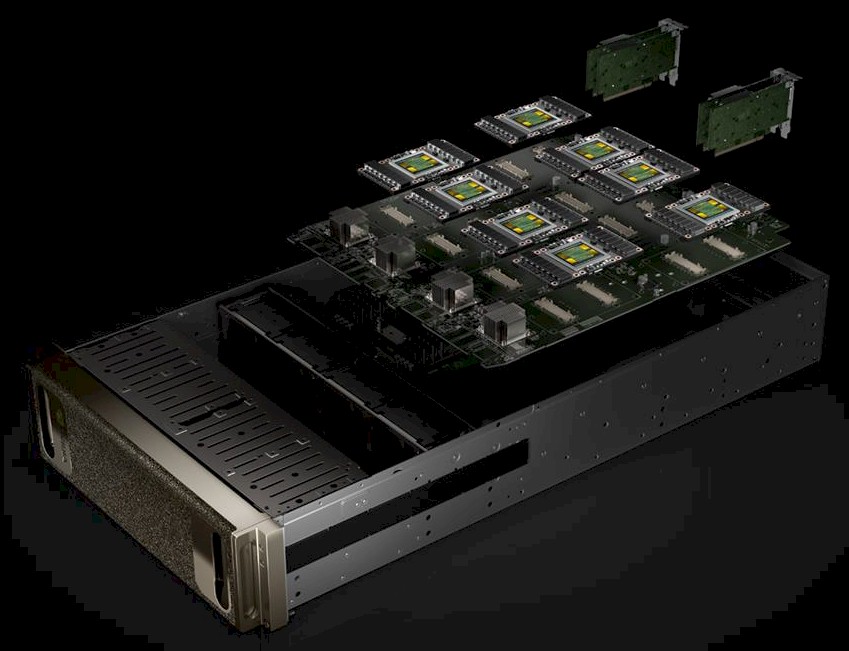
Here is what the HGX GPU complex used in the DGX H100 system from Nvidia looks like:
The NVLink 4.0 ports used on the Hopper GPUs delivered 900 GB/sec of bandwidth, and the NVSwitch ASICs had to be upgraded to provide matching bandwidth across a complex of eight H100 GPUs. This was done with four dual-chip NVSwitch 3 ASICs, which you can see at the front of the HGX chassis in the engineering rendering above.
With the NVSwitch 3 ASIC, Nvidia ported the SHARP in-network computing algorithms and circuitry from its InfiniBand switches to the NVSwitch 3 ASIC, giving it the ability to do certain collective and reduction operations in the network instead of on the DGX node GPUs or ConnextX-7 SmartNICs. Some operations – all reduce, all to all, one to many – naturally belong in the network.
The DHX H100 SuperPOD, which people are still deploying, looks like this:
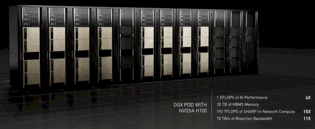
This machine is rated at 1 exaflops at FP8 precision and has 192 teraflops of SHAP in-network processing as well. It also has 20 TB of HBM3 memory across the 256 GPUs in the SuperPOD complex. For those who were being experimental, there was a way to used an interconnect comprised of external NVSwitch 3 switches to create a shared memory GPU complex with all of those 256 GPUs in a SuperPOD coherently linked. That NVSwitch interconnected DGX H100 SuperPOD, as we discussed in detail here, had 6.4X the dense petaflops of performance compared to a DGX A100 SuperPOD, but importantly, at 57,600 GB/sec, had 9X the bi-section bandwidth pf that A100 cluster.
No one, not even Nvidia, did this full NVSwitch-based DGX H100 SuperPOD in production, although this has laid the groundwork for the Blackwell systems.
Which brings us finally to that Blackwell platform:
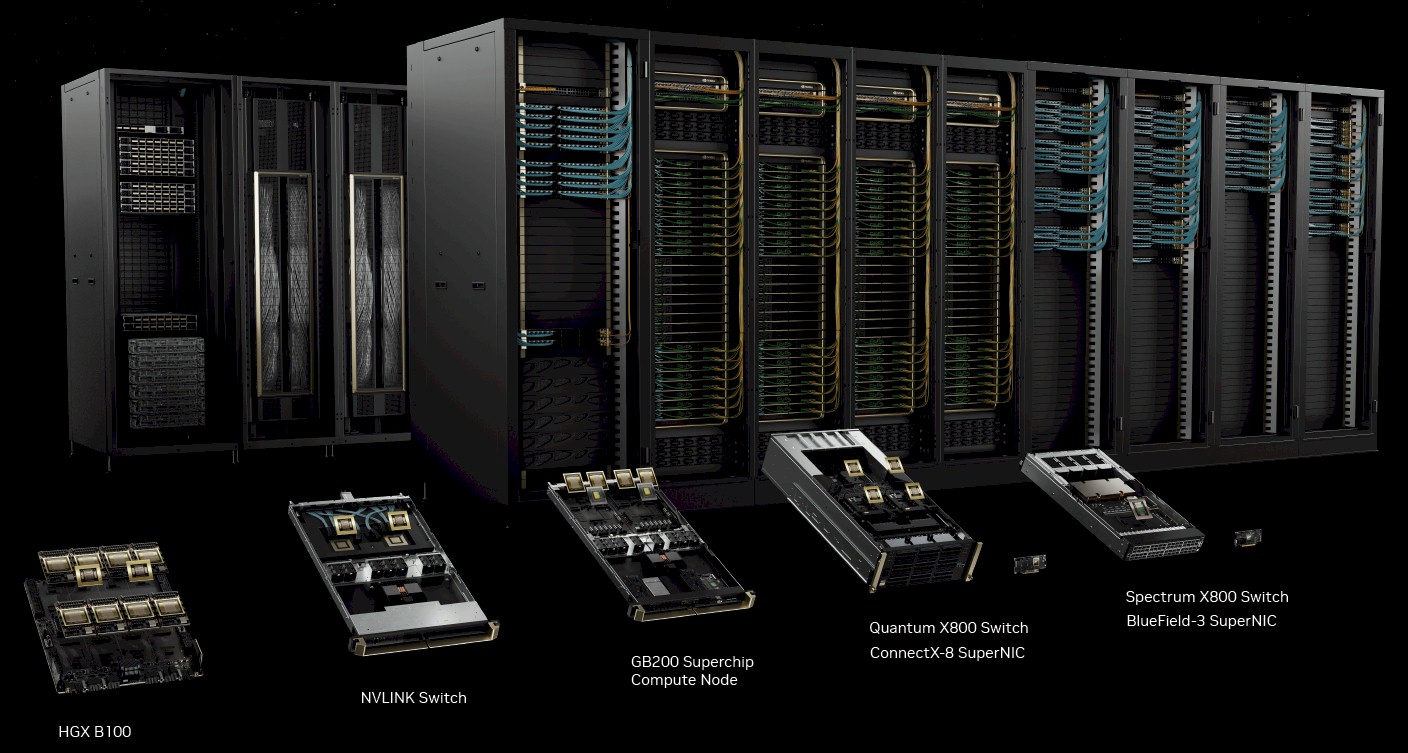
The Blackwell platform starts with the HGX B100 and HGX B200 GPU compute complexes, which will be deployed in DGX B100 and DGX B200 systems and which use geared down variants of the Blackwell GPU that can be air cooled.
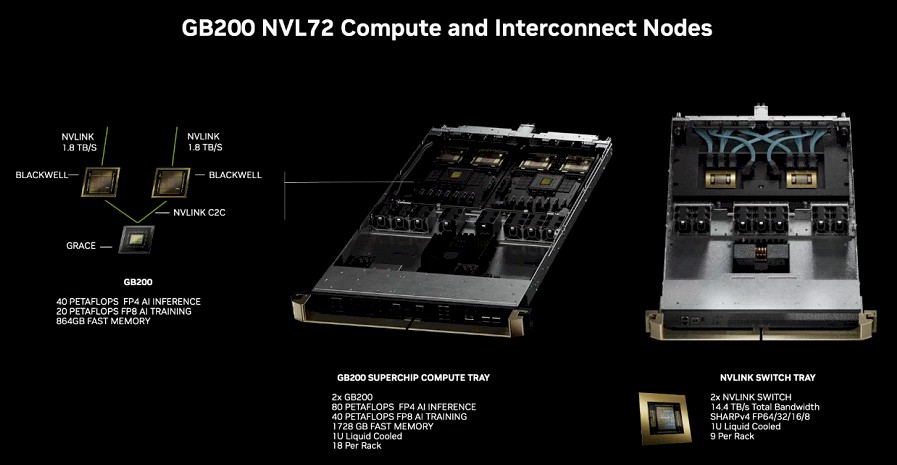
The full-on Blackwell GB100 GPU is being saved for the GB200 Grace-Blackwell SuperPOD, which pairs a single Grace CPU to a pair of Blackwell GPUs that are liquid cooled and used in an NVSwitched system called the GB200 NVL72, which as the name suggests has 72 of the Blackwell GPUs lashed together with an NVSwitch 4 interconnect. This improved interconnect can be scaled to 576 GPUs, which is 2.25X more “scale out” than was available, in theory, on the NVSwitched DGX H100 SuperPOD discussed two years ago.
What this means is a rack with 72 Blackwell GPUs is the new unit of performance that is replacing an eight-CPU node using H100 or H200 or even B100 or B200 GPUs. Not that you will not be able to buy those DGX servers and clones of them from OEMs and ODMs that in turn buy HGX GPU complexes from Nvidia.
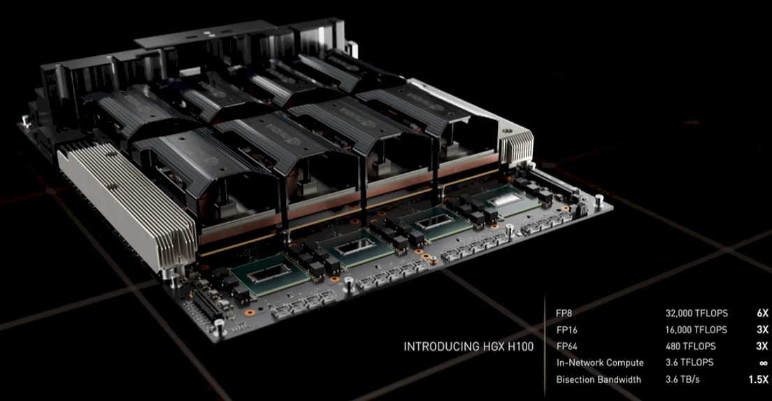
Here are the feeds and speeds on the HGX B100 and HGX B200 and their B100 and B200 GPUs, which are included in the Nvidia Blackwell Architecture Technical Brief:
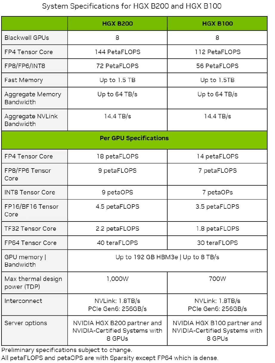
All of the throughput shown at the various precisions and data formats are expressed with sparsity on except the FP64 throughput, which is shown with sparsity turned off.
What immediately jumps out to us is that all data is shown running on tensor cores, not CUDA cores. That doesn’t mean there are no CUDA cores in the Blackwell architecture, but it is odd that they are not shown if they are there – and interesting if there are no CUDA cores. (Our hunch is that there are none, and we are sitting in on an architectural briefing later this evening to find out.)
The other thing that jumps out is all of those “up to” caveats in the memory capacity and memory bandwidth. Don’t be surprised if the B100 and B200 have less than the full 192 GB of HBM3E capacity and 8 TB/sec of bandwidth when these devices are sold later this year. If Nvidia can get manufacturing yield and enough HBM3E memory, it is possible. But clearly Nvidia will want to sell the highest bandwidth and highest capacity HBM3E on the GB200 systems that mix the Grace CPU and a pair of Blackwell B200 GPUs that run full-tilt-boogie in a 1,200 watt thermal envelop each and that deliver the full 20 petaflops at FP4 precision inherent in the Blackwell two-die GPU complex, which we talked about here.
The B100 used in the HGX B100 GPU complexes has the same thermals as the H100 used in the GHX H100 GPU complexes, so any system that was designed for these Hopper H100 SXM5 GPUs can used the Blackwell B100 SXM6 module, which delivers 14 petaflops at FP4 and 7 petaflops at FP8. At FP8 precision, that is 1.8X more throughput per Blackwell die compared to the Hopper die, and there are two of them, which yields a 3.6X increase in FP8 performance. This strongly suggests to us that there are around 2X more tensor cores on the Blackwell die than on the Hopper die.
The B200 used in the HGX B200 GPU complex runs 42.9 percent hotter and delivers 18 petaflops per two-die socket at FP4 precision. With 9 petaflops at FP8 precision with sparsity on per Blackwell die running at whatever speed the B200 is running at, that is 2.25X more oomph than the H100 chip and there are two of them, which yields 4.5X more performance per socket.
Making One Ginormous GPU
One new component in these HGX B100 and HGX B200 systems is the NVLink 5 port and the NVLink Switch 4 ASIC, which the ports on the GPUs talk to. Both have SerDes circuits that run at 100 Gb/sec signaling per lane and with PAM-4 encoding, which carries two bits per signal, that drives the effective bandwidth to 200 Gb/sec per lane. Lanes are massively aggregated to deliver 1.8 TB/sec of bi-directional bandwidth out of the ports on the B100 and B200 GPU complexes and into and across the NVLink Switch 4 (what we sometimes just call NVSwitch 4) ASIC. That NVSwitch 4 ASIC has 7.2 TB/sec of aggregate bandwidth, which means it can drive a total of four 1.8 TB/sec NVLink ports. (That is an incredible 72 lanes running at 200 Gb/sec for each port.)
The SerDes on this ASIC drive 72 ports running at 200 Gb/sec, and they are the same SerDes that are being used in the new InfiniBand Quantum-X800 (formerly known as Quantum-3), which has 115.2 Tb/sec of aggregate bandwidth and can drive 144 ports running at 800 Gb/sec speeds.
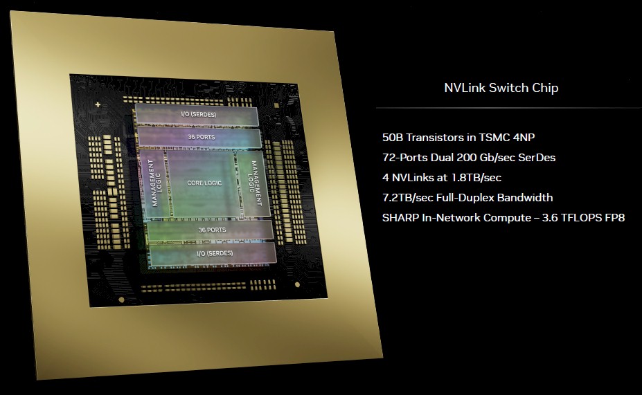
Here is a zoom in on the NVLink Switch 4 die:
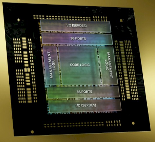
This chip has 50 billion transistors and is implemented in the same TSMC 4NP process that is used for the Blackwell GPUs.
The new NVLink Switch has 3.6 teraflops of SHARP v4 in-network computing for doing collective operations inside of the switch, which boosts the efficiency of GPU clusters. Some collective operations that are done in parallel calculations, particularly calculating average weights and delivering them at an intermediary stage of a calculation, are best performed in the network, which is at a local center of the nodes that it connects to.
Interestingly, the NVLink Switch 4 ASIC can provide a confidential computing domain across 128 GPUs, and can scale the NVLink coherent memory fabric across a maximum of 576 GPUs, the latter of which is 2.25X larger than the 256 CPU theoretical memory fabric scale with the NVLink Switch 3 ASIC. Ian Buck, general manager of hyperscale and HPC at Nvidia, cautions us that just like that 256 GPU limit was a theoretical one, meant for research not production, with the NVLink Switch 3, that 576 GPU maximum for NVLink Switch 4 is also meant for research, not production.
However, this time around, as expressed in the GB200 NVL72 system that we will now walk through, 72 GPUs that are sharing GPU memory in a tight coupling is the new unit of compute, like eight or sixteen GPUs have been since the advent of the DGX line of systems and their HGX GPU complexes and NVSwitch interconnects. What was once a node is now a full rack. And frankly, it is about time.
Here are the components in the rack:
That 2:1 ratio of GPUs to CPUs shows that having Grace be so powerful was not necessary for AI hosts, and even the adjunct LPDDR5 memory was not needed as much as it is for the embeddings that are used for recommendation engines. Grace only has a 600 GB/sec NVLink 4.0 port coming out of it, and this is split into two, using 300 GB/sec to chat to each Blackwell B200 GPU. That’s a lot more than PCI-Express can do, and in fact, it will be early next year before we have 256 GB/sec PCI-Express 6.0 x16 slots. The 1.8 TB/sec bandwidth that Nvidia will deliver this year with NVLink 5.0 ports won be available until around 2032 with PCI-Express 9.0 x16 slots delivering 2 TB/sec at that time.
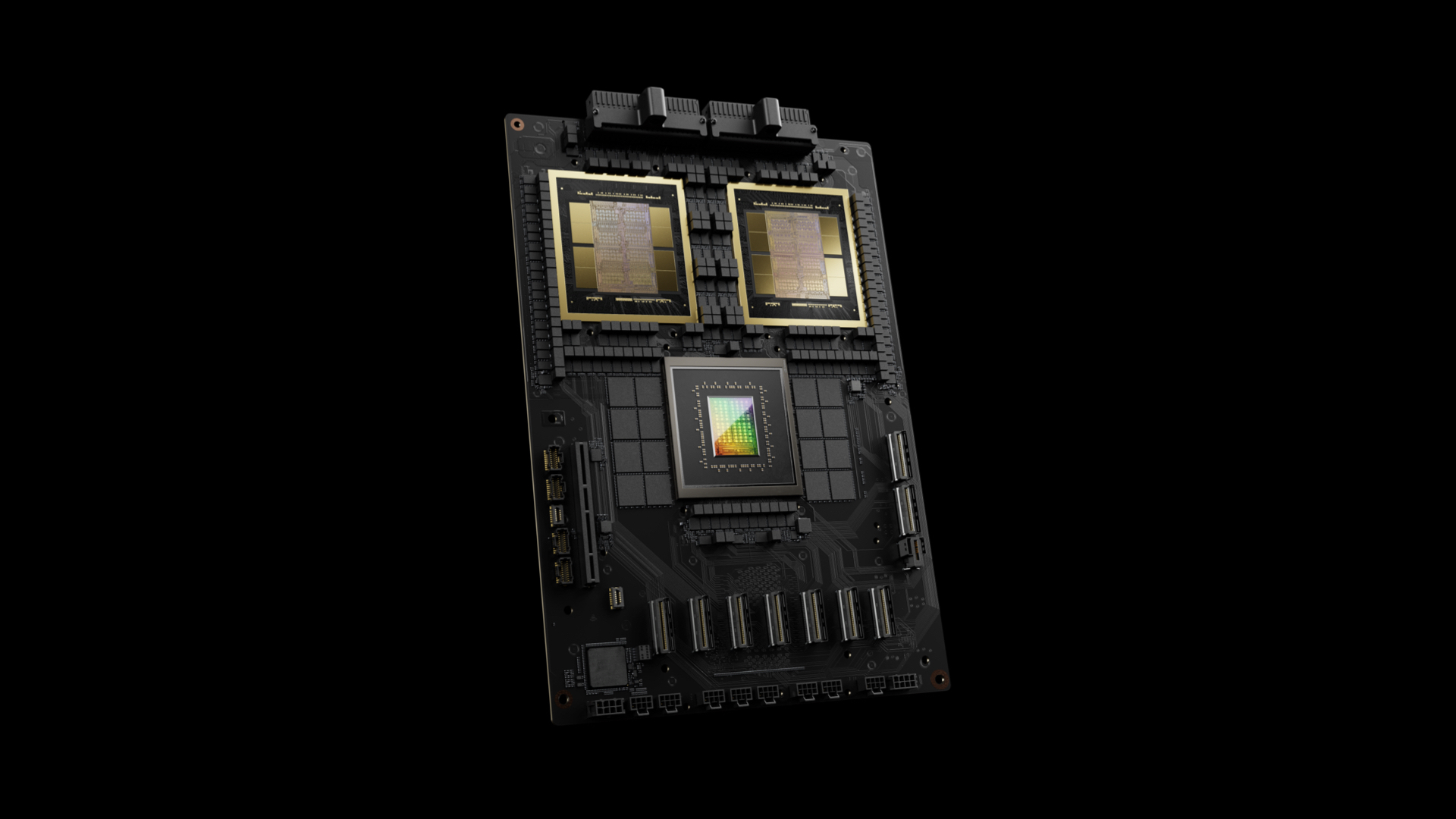
Here is a zoom on that Grace-Blackwell superchip:
And here is what the DXG GB200 NVL72 rack system looks like:
The front of the rack is on the left and the back of the rack, with miles of copper cable, is on the right.
This rack is the new unit of compute, and the reason why is simple: At these NVLink Switch bandwidths, a rack is as far a distance between components that can still be interconnected with copper wires and not have to switch to retimers, optical transceivers, and fiber optic cables. Go much further than a rack and you have to move into the realm of optics, which adds cost and heat – and a lot of both. It is a think we hear again and again in system architecture.
“So this is what makes it possible,” explained Nvidia co-founder and chief executive officer Jensen Huang as he did a buildup and teardown of the Blackwell rackscale design. “That’s the back, the DGX NVLink spine, and 130 TB/sec goes to the back of that chassis – that is more than the aggregate bandwidth of the Internet, so we can basically send everything to everybody within a second. And so we have 5,000 NVLink cables – in total two miles. Now this is the amazing thing. If we had to use optics, we would have had to use transceivers and retimers, and those transceivers and retimers alone would have cost 20,000 watts – 2 kilowatts of just transceivers alone – just to drive the NVLink spine. We did it completely for free over NVLink Switch and we were able to save the 20 kilowatts for computation. This entire rack is 120 kilowatts, so that 20 kilowatts makes a huge difference.”
And the cost of the mix of copper and optical network links would raise the cost of the NVLink Switch fabric by a factor of 6X, according to Buck. And that is why, we surmise, that anything beyond 72 GPUs is still going to be for research, not production, and that these racks will be interlinked with InfiniBand or Ethernet, not NVLink Switch, unless you have a lot of money to spare for power, cooling, and optics.
Foreshadowing Is How You Tell Literature From Cheap Pulp
This rackscale approach embodied at the top-end of the Blackwell platform was foreshadowed in the “Ceiba” supercomputer being built by Nvidia and Amazon Web Services that we told you about back in November. That Ceiba machine was based on what is called the DGX GH200 NVL32, and as the name suggests, it was a rackscale design based on NVLink Switch 3 interconnects that connected 32 of the Grace-Hopper CPU-GPU superchips together into a shared compute complex It had nine NVSwitch systems to interlink those compute engines and delivered 128 petaflops, 20 TB of total memory (4.5 TB of that was HBM3E with a total of 157 TB/sec of aggregate memory bandwidth), all linked by 57.6 TB/sec of aggregate NVLink bandwidth.
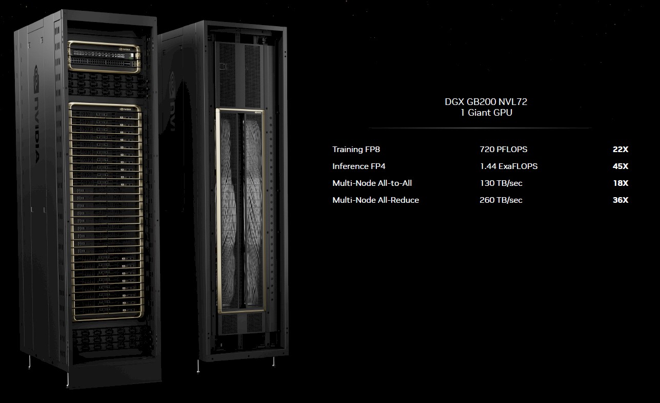
The Blackwell GB200 NVL72 takes the Ceiba approach to a whole nuthah level, as we say in New Jersey.
The chart above shows the multiples for the GB200 NVL72 compared to a DGX H100. But that is not the real comparison.
The one to compare, as Huang walked through during his keynote, was how to train the 1.8 trillion parameter GPT-4 Mixture of Experts LLM from OpenAI. On a cluster of SuperPODs based on the Hopper H100 GPUs using InfiniBand outside of the node and NVLink 3 inside of the node, it took 8,000 GPUs 90 days and 15 megawatts of juice to complete the training run. To do the same training run in the same 90 days on the GB200 NVL72, it would take only 2,000 GPUs and 4 megawatts. If you did it across 6,000 Blackwell B200 GPUs, it would take 30 days and 12 megawatts.
This is not really a computation issue as much as it is an I/O and computation issue, Buck explained to us. With these Mixture of Expert modules, there are many more layers of parallelism and communication across and within those layers. There is the data parallelism – breaking the data set into chunks and dispatching parts of the calculation to each GPU – that is the hallmark of HPC and early AI computing. Then there is tensor parallelism (breaking a given calculation matrix across multiple tensor cores) and pipeline parallelism (dispatching layers of the neural network processing to individual GPUs to process them in parallel to speed them up). And now we have model parallelism as we have a mixture of experts who do their training and inference so we can see which one is the best at giving this kind of answer.
It hurts to think about it, and you need an AI to keep track of it all probably. . . . Buck says that to figure out the right configurations of parallelism to run GPT-4 training on the GB200 NVL72 cluster, Nvidia did more than 2,600 experiments to figure out the right way to create the hardware and dice and slice the model to make it run as efficiently as possible. Here are some of those experiments, plotted out:
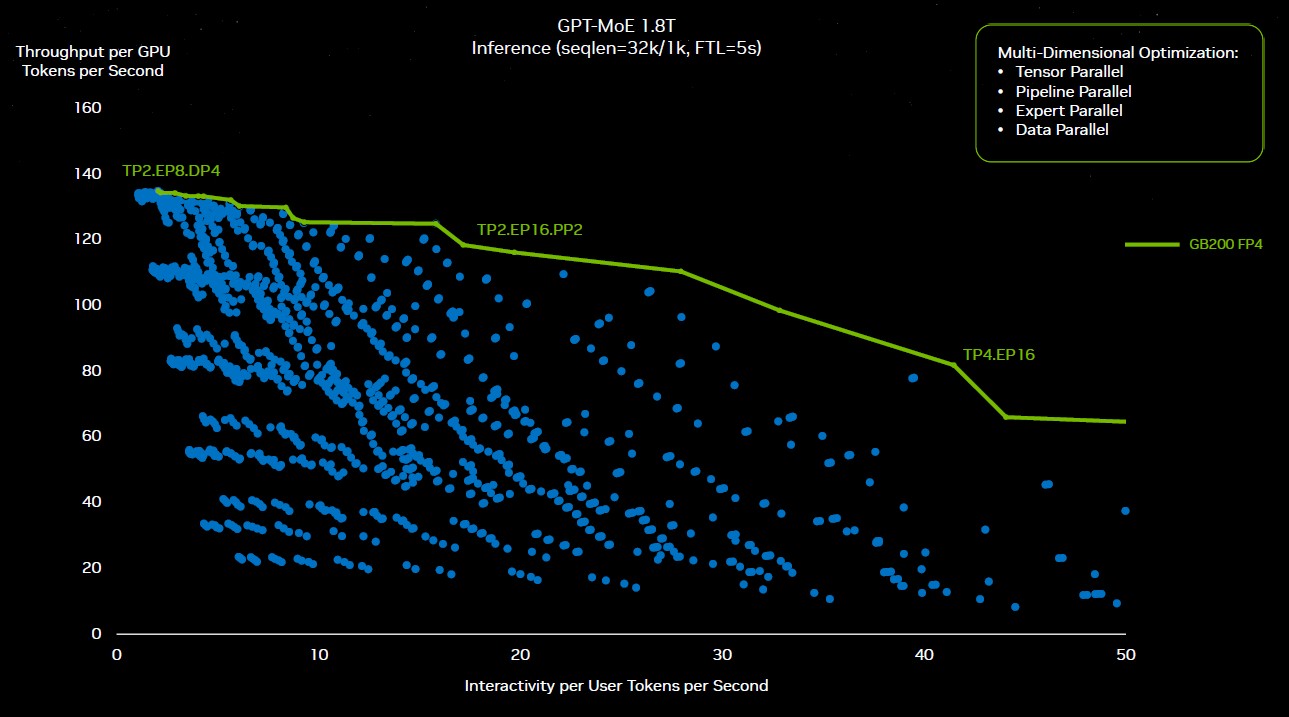
“All those blue dots came from some repartitioning of the software,” explained Huang in his keynote. “Some optimizing solution has to go and figure out whether to use tensor parallel, expert parallel, pipeline parallel, or data parallel and distribute this enormous model across all these different GPUs to get the sustained performance that you need. This exploration space would be impossible if not for the programmability of Nvidia’s GPUs. And so we could, because of CUDA, because we have such a rich ecosystem, we can explore this universe and find that green roofline.”
Now, here is how the Hopper and the Blackwell rooflines look working on GPT-4 MOE at 1.8 trillion parameters, and just for fun, there is a theoretical Blackwell line in purple in the middle that shows how Blackwell would have done if it was just put together in a cluster mixing NVLink Switch 3 and 400 Gb/sec InfiniBand as the Hopper systems were done and stuck with FP8 precision and did not move to the new Transformer Engine and FP4 processing for inference. A kind of simple silicon upgrade but not a system upgrade:
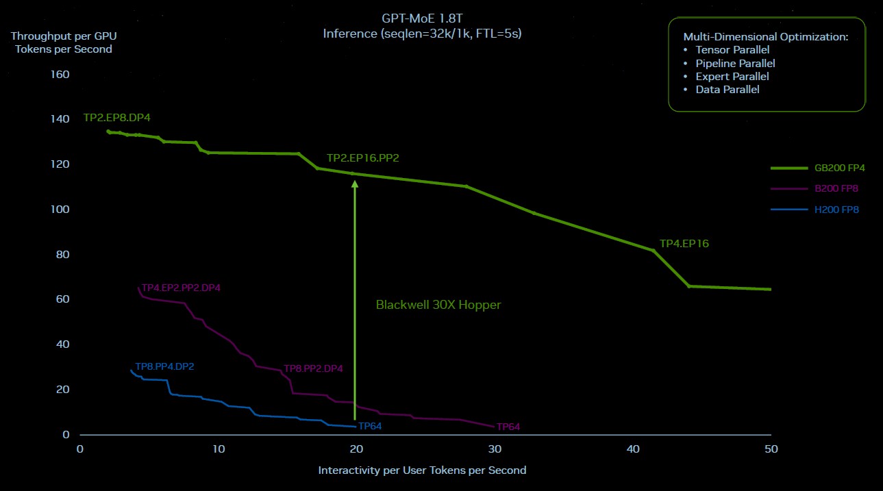
Clearly, just doing a rough upgrade to Hopper to make Blackwell was not the answer. And all of the things that improve inference performance by 30X and reduce inference power consumption by 25X, as Nvidia is claiming, were the right moves.
There are a lot of simultaneous effects at work here. Running this GPT-4 MOE model on a cluster of only sixteen Hopper-class GPUs – two HGX boards interlinked with InfiniBand – because of the collective operations across the levels of parallelism, about 60 percent of the wall time for the machine was used in communication and only 40 percent was only used for compute. The faster and fatter NVLink Switch interconnect is allowing more of that compute to be used.
With the NVLink Switch interconnect across 72 GPUs, those GPUs can talk incredibly fast to each other – and they can all talk to each other at the same time when necessary and complete that chatter fast. Not only that, there are two GPUs in each node GB200 node, instead of only one GPU per node with the GH200 node. There is roughly twice as much HBM3E memory per GPU and almost twice as much bandwidth. In the liquid cooled GB200 NVL72 configuration, those two Blackwell sockets have 40 petaflops of FP4 oomph, compared to 4 petaflops of FP8 oomph for the one Hopper socket.
The networking is clearly as important as the compute.
Eight of these GB200 72NVL racks now comprise a SuperPOD, by the way, and you can interconnect them with 800 Gb/sec InfiniBand or Ethernet or go experimental and link all of the 576 GPUs in that half row of racks to create a much larger shared memory system. The latter will probably have a networking bill that is almost as big as the compute bill. But, with a 576-GPU memory and compute domain, it might be worth it. . . . Some years hence, the row will be the new node, after all. Like two years from now, based on current trends. And soon after that, the datacenter will be the new node.


Happy Spring Equinox (and Cherry Blossoms) to all!
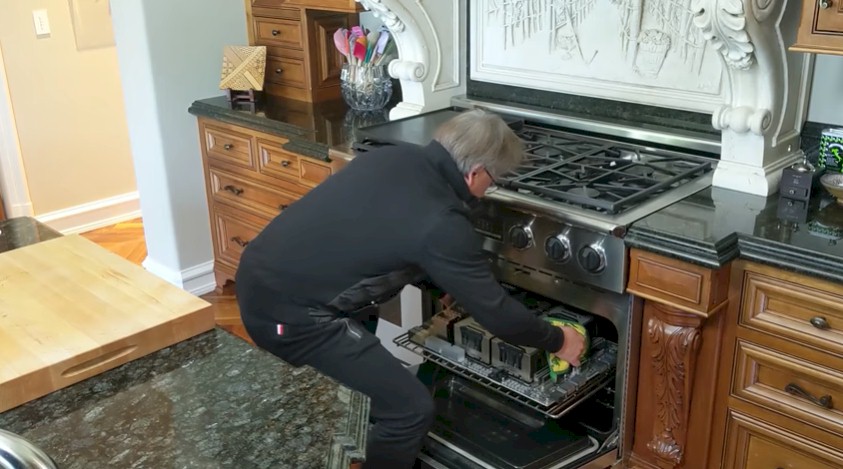
With these upgrades, It looks like they can now pretty-much make an MS Eagle-equivalent machine (Top500 #3) with an 8×8 array of DXG Grace-Blackwell GB200 NVL72 racks … which is impressively compact! No wonder Jensen can bake them in his home’s kitchen oven! (eh-eh-eh!)
About memory coherence, this has been an industry debate (fight?) for more years than I care to remember. Mellanox (pre-acquisition) has always been marketing the benefits, but always fell short on the specifics of why it mattered to (standard) software. Sure, simplification of the programming model for pointer chasing – but ignorance of the physical topology in commercial (or research for that matter) has time and time again shown the limits.
Perhaps now that NLV72 is more of an appliance with somewhat of a singular workload (vs. trying to optimize for DB / Web / HPC….) coherence will showcase the market pull use case vs. the technology market push inventions. Are we saying the in-net reduction operations (“collections” as Jensen referred to them) are the killer app?
TPM does the absolute best in his writing, and asks the hard questions that hold technology peddlers proverbial feet to the fire to explain why their proposed value matters to customers. I was involved in CAPI, CCIX, but thankfully not Gen-Z. I hold patents in cloud and RDMA technology inventions. This is coming from a place of intimate knowledge.
Timothy, I humbly submit to you a request to deep dive on coherence (which to some extent would be an update from Nov 23, 2021 “FINALLY, A COHERENT INTERCONNECT STRATEGY: CXL ABSORBS GEN-Z”). I think the consumers of this tech needs the answers from a knowledgeable neutral party that can interrogate vendors, software developers/ISV’s on why memory coherence matters. I hope the answer isn’t “because CSP’s requested it to help their memory disaggregation dreams come true” as that dog just doesn’t TCO hunt.
Respect.
I have been told in the past that I over-value coherence, and I have tried to not think the coherency domain should be the size of a datacenter. Which would be my natural inclination. (Smile) Very good points above, and I will take this as an assignment.