
We are still plowing through the many, many presentions from the Hot Interconnects, Hot Chips, Google Cloud Next, and Meta Networking @ Scale conferences that all happened recently and at essentially the same time. And we intend to take our usual, methodical approach of finding the interesting bits and doing some analysis on what we have heard and seen.
This time around, we are looking at the formal launch of the “Demeter” Neoverse V2 core by soon-to-be-re-publicked Arm Ltd.
Had the Demeter core design happened five years ago, or better still ten years ago, this would have been a very big deal because designing good cores was very tough for a lot of organizations who wanted to make Arm server chips. And as the “Genesis” Compute Subsystem (CSS) announcement also from Hot Chips this year shows, maybe it is also difficult to design a good processor. Rather than design processors, what the hyperscalers and the cloud builders have always wanted to do is heavily customize processors for their workloads. Large enterprises sometimes want this too, and classes of enterprises of all sizes as groups with specific workload needs also want this.
But processor sellers (not all sellers are makers and not all makers are sellers) have been unable to provide mass customization because it is very expensive to make more than a couple of variations with each generation. The variations we do see are really about turning features on and off that are inherent in a few designs, and this is compelled by yields on sections of the silicon as it is by power gating features to artificially create variations and charge premiums for parts.
The Demeter core, which is the first one to implement the Armv9 architecture announced way back in March 2021, is by far the best one that Arm has ever designed for servers, and that is why Nvidia was able to just license this core and other components for its 72-core “Grace” server CPU, which is integral for Nvidia’s system architecture to support all-CPU computing for traditional HPC simulation and modeling workloads as well as providing auxiliary memory and compute capacity. With four 128-bit SVE2 vector engines, the Demeter core will certainly have a capable engine for running classic HPC workloads as well as certain AI inference workloads (those that aren’t too fat, and probably not including most LLMs) and maybe even the retraining of AI models in certain cases. And with somewhere between 16 and 256 cores possible in a design, the flops can certainly be stacked up.
We just wonder who else other than Nvidia is going to use the Demeter core in their CPU designs.
AWS will very likely employ the V2 core in its future Graviton4 homegrown server processor and which uses the “Zeus” V1 core in its current Graviton3 processor. Alibaba is using the Neoverse “Perseus” N2 cores in its homegrown 128-core Yitian 710 processor, and it could switch to the V2 core in a follow-on Yitian chip if it sees a need to support more vector and matrix math in standard servers given the increasing use of AI algorithms, which are heavy on such math. HiSilicon, the chip design arm of Huawei Technologies, uses the Neoverse “Ares” N1 core from Arm in its 64-core Kunpeng 920 server chip, and it could do a follow-on with the V2 core for the same reasons. It is not known what cores Google is using in the pair of custom Arm server chips that it is rumored to be working on – one in conjunction with Marvell, one with its own team if the scuttlebutt is true – but we would not be surprised if one of them is using the V2 core. Ampere Computing has switched away from the “Ares” N1 cores from Arm to its own core (what we call the A1) in its 192-core “Siryn” AmpereOne chip. The Center for Development of Advanced Computing (C-DAC) in India, which is building its own “Aum” processor for HPC workloads, and it is based on Arm’s Neoverse V1 core. And as we have pointed out before, the 512-bit vectors in the custom Arm cores created jointly by Fujitsu, Arm, and RIKEN Lab in Japan for the 48-core A64FX processor used in the “Fugaku” supercomputer can be considered a kind of Neoverse V0 core in that the SVE design was first created for the A64FX.
We also wonder why there was not immediately a CSS server chip design available based on the V2 core in addition to the N2 core chip that Arm unveiled at Hot Chips 2023. Why not both N2 and V2 cores in CSS designs at the same time? We realize that some datacenter operators need more optimizations for price/performance and don’t think they need as many vectors; it remains to be seen by the software and the workloads if they are right. But AWS choosing the V1 and Nvidia choosing the V2 is a pretty strong indicator. The Ampere Computing A1 core is more like an N2 core with regards to its vectors, having two 128-bit engines, so this behavior of fat-vectored cores on the cloud is not universal.
V2 Is Like A Rocket
Arm trifurcated its Neoverse core and CPU designs in September 2020, splitting the V series high performance cores (with doubled-up vector engines) from the mainline N series cores (with a focus on integer performance) and added in the E series (entry level chips with a focus on energy efficiency and the edge). The roadmap has been expanded and updated a bunch of times over the years, and the latest one, with the CSS subsystem variant of the N2 platform add, was presented at Hot Chips:
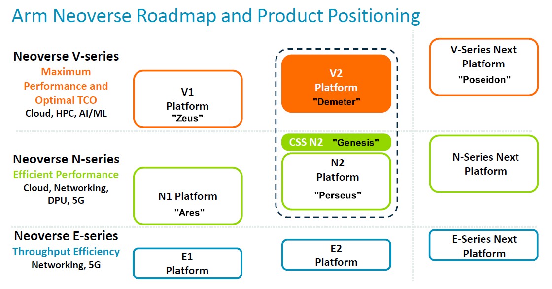
We added in the core and platform codenames where we knew them because we like synonyms.
Magnus Bruce, Arm Fellow and lead CPU architect, walked through the V2 platform at Hot Chips, talking about the architecture and about the changes from the Zeus V1 platform. This chart summarizes it nicely:
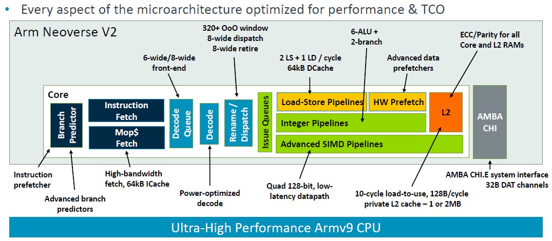
“The foundation of this pipeline is a run-ahead branch predictor, and this branch predictor acts as an instruction prefetcher and it decouples fetch from branch,” explained Bruce. “Large branch prediction structures provide coverage of very large real life server workloads. We use physical register files that are read after issue, allowing for very large issue queues without the burden of storing data. This is necessary to unlock ILP [instruction level parallelism]. We use low latency and private L2 caches, low latency L1 and private L2 caches with state of the art prefetching algorithms and aggressive store-to-load forwarding to keep the cores fed with minimal bubbles and stalls. Dynamic feedback mechanisms from the system allow the cores to regulate aggressiveness and proactively prevent system congestion. These fundamental concepts are what allow us to push width and depth of the machine while maintaining the short pipeline necessary for quick mispredict recovery.”
The important thing is that this is an Armv9 implementation and it is meant to shake out that architecture and, which brings performance, security, and scalability enhancements compared to the many generations of the Armv8 architecture that has defined Arm chips for over a decade.
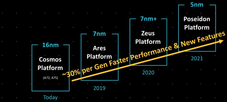
The architectural tweaks with the V2 chip are subtle, but clearly effective. But also clearly, the 13 percent performance improvement is a long way from the 30 percent instruction per clock (IPC) improvement goal that Arm itself set way back in 2019:
Anyway, here is a drilldown on the branch predictor and fetch units and the L1 caches for the V2 core:
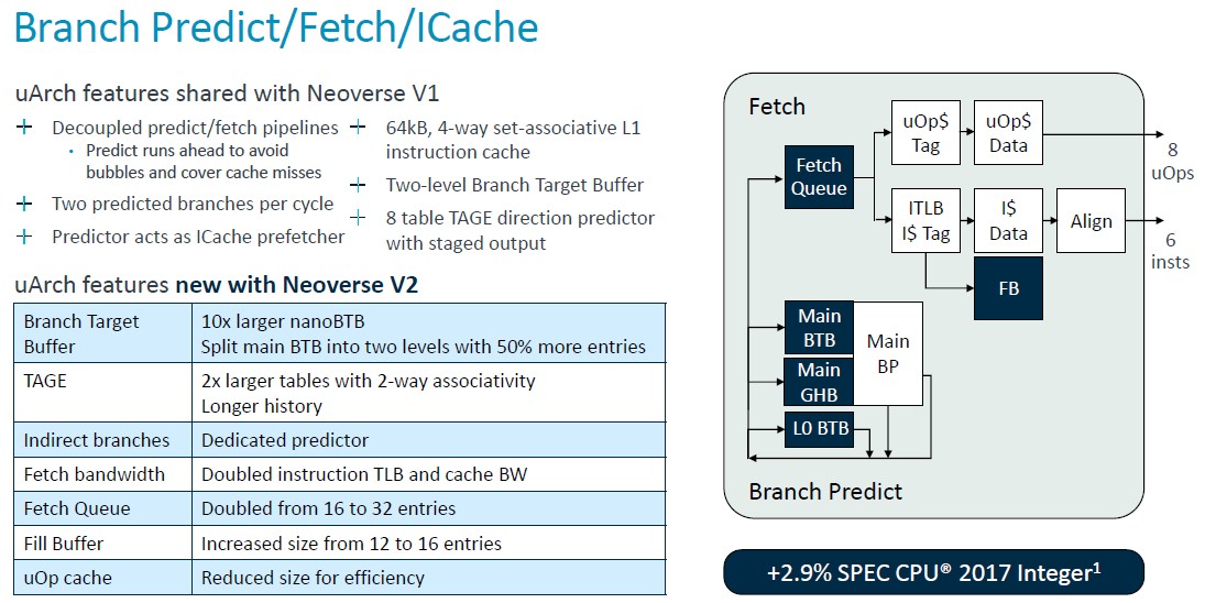
As you can see, a lot of the features of the V1 core are moved over to the V2 core, but the V2 core also has some updates. Lots of queues, tables, and bandwidths were doubled, but the micro-op cache was actually reduced in moving to the V2 design. Thes tweaks to the V2 core added about 2.9 percent more instructions per clock based on modeled SPEC CPU 2017 integer benchmarks for the V1 and the V2 using chip simulators.
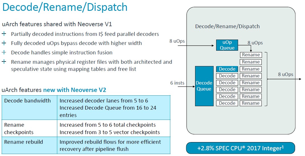
Once again, some of the microarchitecture goodness of the V1 core with regards decoding and dispatching of instructions to was passed straight through to the V2 core, but decoder lanes and queues were boosted a bit. The overall effect was a 2.9 percent increase in IPC, again gauged by the SPEC CPU 2017 integer test. (IPC is generally calculated using a mix of tests, not just SPEC CPU ratings. But this is what we got.)
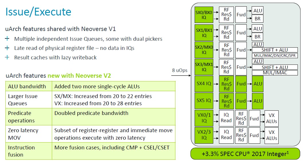
With the V2 core, Arm architects added two more single-cycle arithmetic logic units (ALUs) and increased the sizes of the issue queues and doubled the bandwidth on the predicate operators, and these tweaks, with a bunch of others, added another 3.3 percent to the performance of the core normalized at 2.8 GHz.
As with the V1 core, the V2 core has two load/store pipes and one load pipe, but the entries on the table lookaside buffer (TLB) were boosted – from 40 entries to 48 entries – and the various store and read queues were also made larger.
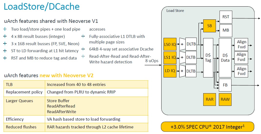
This and other changes added another 3 percent increase in the V2 core oomph.
Arm architects got their biggest increase in performance from changes in the hardware prefetching for data:
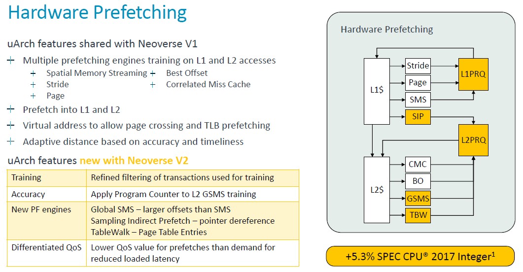
“The Neoverse V1 already had state of the art prefetching,” explained Bruce, and we are going to let him walk you through this low level explanation of the prefetching enhancements. Take a deep breath. . . . “Using multiple engines training on L1 and L2 misses and prefetching into both L1 and L2 caches, our prefetchers generally use virtual addresses to allow page crossing – and this allows them to act as TLB prefetches as well. The prefetchers use dynamic feedback from the interconnect, as well as accuracy and timeliness measurements inside the CPU, to regulate their aggressiveness. The V2 builds on the V1 hardware by improving training, improving accuracy through better filtering and training operations, and making use of the program counter in more prefetchers for better correlation and better prevention of aliasing. New prefetching engines are also added. The L2 gains global spatial memory streaming engine that increases the range of offsets of the prefetcher that it can cover, and it greatly improves over the older standard SMS engine. We add a sampling indirect prefetcher, which handles pointer dereferencing scenarios. It’s not data prediction, but it is learning patterns of data consumption as pointers for other loads. We also add a table walk prefetcher that enables prefetching of page table entries into the L2 cache. Now, all of these added prefetchers and their aggressiveness can create congestion in the system. Particularly at shared resources like the system level cache or DRAM. We provide differentiated QoS levels for demands and prefetches. And that allows us to have aggressive prefetching without hurting the loaded latency of demand requests. Dynamic prefetching dynamic feedback regulates prefetcher aggressiveness to a sustainable level. These changes combined for 5.3 percent increase in spec manager, but more importantly, we see an 8.2 percent reduction in SLC misses at the same time, so we gain more performance with less DRAM traffic.”
Here is how that L2 cache works its magic:
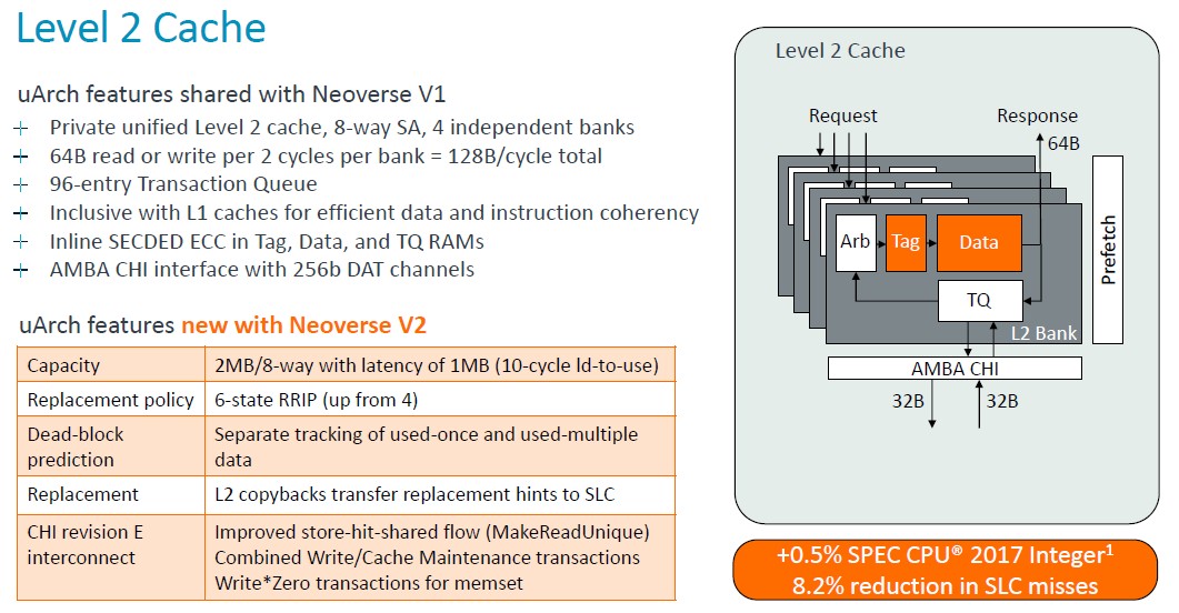
Not a big change in performance from the L2 cache being doubled, but that reduction in system level cache misses does boost performance indirectly.
Here is how the IPC all adds up:
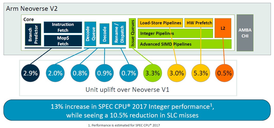
These are additive, not multiplicative, effects, and the V2 core has a 13 percent increase in integer performance – again, this is modeled and, again, this is only using the SPEC CPU 2017 integer test – while reducing system level cache misses by 10.5 percent overall.
Whenever a new core or chip comes out, that core or chip is graded on how performance, power, and area interplay. Here is how the V1 and V2 cores stack up:
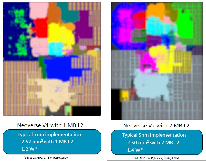
The V1 core implemented in a 7 nanometer process had 2.5 square millimeters of area with 1 MB of L2 cache and burned about 1.2 watts. The V2 core has a tiny bit less area with twice the L2 cache at 2 MB, and boosts the power draw by 17 percent. These comparisons are all normalized to 2.8 GHz clock speeds.
And of course, the V2 is not just a core, but a platform specification that can be licensed:
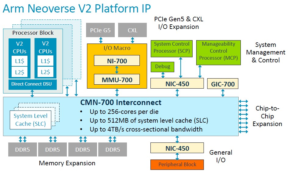
With the CMN-700 interconnect, Arm licensees can build a V2 CPU that can scale to 256 cores and 512 MB of system level cache, with that interconnect supplying 4 TB/sec of cross-sectional bandwidth across all of the cores, memory, and I/O controllers that sit on the mesh.
A lot of the presentation for the V2 core focused on integer stuff, but in the Q&A for the talk, Bruce did say something interesting about vector performance. The V1 core had a pair of 256-bit SVE1 vector engines, but the V2 core has a quad of 128-bit SVE2 vector engines. This was done, as Bruce put it, because it was easier (and we presume more effective) to spread mixed precision math over four units than it was to try to do it over two units.
But as we say, other than Nvidia and possibly AWS, who is going to license the V2 core? Maybe anyone who is going to use V2 is already doing a custom design and therefore there is no reason to make a CSS variant?

The AI Wave Finally Starts Lifting Dell And HPE
It is beginning to look like the Dell Technologies and Hewlett Packard Enterprose, the world’s two biggest original equipment manufacturers, are finally going to start benefitting from the generative AI wave, mainly because they are finally getting enough allocations of GPUs from Nvidia and AMD that they can start addressing …
Broadcom And Marvell Ride The Compute Engine Independence Wave
Nvidia sells the lion’s share of the parallel compute underpinning AI training, and it has a very large – and probably dominant – share of AI inference. But will these hold? This is a reasonable question as we watch the rise of homegrown XPUs for AI processing by the hyperscalers …
The Prospects For An Arm Server Insurrection
If you want to break into datacenter compute in a sustainable way, it takes the patience of a glacier. And not just any glacier, but one that predates the Industrial Revolution. The reason is that IT shops are a conservative lot, and change comes slowly, even when they seem to …
Wow! That’s the deepest of deep drilldowns I’ve seen in quite awhile (a Whopper!)! My answer to the title survey question is (of course): everyone will use the Neoverse V2! HPC and AI will want to add HBM though, as found in A64FX (Neo. V0), SiPearl Rhea (Neo. V1), and on the GPU part of the GH200 (Neo. V2 for the CPU part).
There’s some indication that the V0 to V2 progression is meant to make the CPU more nimble and agile (more responsive, less crampy and sclerotic) as it jumps around through code and data. For example, the width of vector units went down from 2x512b in “V0”, to 2x256b in V1, and 4x128b in V2. This should also help with chip layout (cost), and power consumption (cost). Also, the A64FX/V0 has 256-byte cache lines, vs the more normal 64B for V1 & V2 (more nimble). The L2 cache per core increased from 0.67MB in V0, to 1MB in V1, and 2MB in V2, which is generally great as well (thanks to 5nm vs 7nm). And, in V2, they do “aggressive store-to-load forwarding [for] minimal bubbles and stalls […] maintaining the short pipeline […] for quick mispredict recovery.” (more nimble).
As the article suggests, the impact of these improvements should almost not show up at all in Spec CPU (a benchmark of ALU/FPU perf with blocky memory transfers, if any), but they should be much more visible in workloads with scattered memory accesses and when running virtual machines (and dynamic languages like Python and Javascript). In other words, V2 is the right direction for datacenter servers, HPC, and AI. Next-up, they’ll want to reduce the size of cache lines to 32B (for graphs!), in V3.
It’s fun to see that, even in ARM’s RISC (since Cortex-A78?), instructions can be split internally into μOps, and/or fused into MOps (eg. CMP + CSEL/CSET in the Issue/Execute slide), for increased performance!
I’m not sure why V2 adds those 2 ALUs when there were 6 already in V1 (maybe for speculative execution in crazy-branched code, or 3 levels of binary branches in the execution tree/graph, a bit like chess?), but looking at FP64 efficiency it looks like 16 GF/W (8 x 2.8 GHz / 1.4 W) which is Fugaku-like (15.4 GF/W). As with other CPUs then, pairing with accelerators seems needed to get to the 100+ GF/W of MI300A and H100.
Maybe, for HPC/AI, they could remove the 2 extra ALUs, and cut L2 back to 1 MB, and use the freed space for a couple 4×4 or 8×8 matrix units?
Inasmuch as speculative execution is a hardware implementation of McCarthy’s ambiguous operator (amb), with branch-predictor heuristics to prioritize moves (as in chess), the more execution ports are available to run this in parallel, the better — so I’d vote to keep V2’s new ALUs (I think).
I might agree with you on cutting per core L2 back to 1MB and increasing FP64 oomph instead, say with 4x or 8x 256-bit vector units, to provide one or two single-cycle 4×4 FP64 matmuls, and fit the nimbler 32B line size. It should be tested for performance and efficiency though.
… or, seeing how these V2 cores are so tiny at 2.5 mm^2, AMD could bake 96 of them in a pair of tasty chiplets, plunk them onto an MI300N (N for Neoverse) with 4 Instinct GPU dies, and then make some funny faces at NVIDIA! d^%^p