
It takes too long to get a new compute engine in the field, and everybody complains about it. Customers are impatient because they want more performance and the better bang for the buck that always comes with a new generation of chips. And those who make CPUs, GPUs, and other compute engines are impatient, too. They want to crush the competition and make more money.
At Hot Chips 2023 this week, when Arm Ltd was showing off its “Demeter” V2 cores just after announcing it was going public (again), the company also rolled out the “Genesis” N2 Compute Subsystems, or the CSS intellectual package for short. (We will be covering the V2 core deep dive separately.) This Genesis effort has a chance of getting Arm CPUs into the field faster than has been possible in the past.
Over the years, Arm has been inching closer and closer to putting together full-blown CPUs for customers to modify and take straighter to market. Back in the late 2000s, when Arm had taken over smartphones and server makers were thinking about how the Arm architecture might improve upon an X86 architecture that was essentially a monopoly, server chip designers started out with an Arm architecture license and had at it. This was a very expensive and time-consuming way to create a server chip, albeit better than starting with a custom ISA, which the world would have no tolerance for because of the massive software porting job.
After many failed Arm server chip attempts – by both established semiconductor giants like Broadcom, Qualcomm, AMD, and Samsung as well as startups like Calxeda and Applied Micro – and some limited success by Cavium with its ThunderX and ThunderX2 CPUs, Arm decided to make it a little bit easier with its Neoverse effort, which was rolled out in October 2018 and which provided not only a roadmap for server chip cores, but reference architectures for turning these into proper CPUs with a mixture of other Arm intellectual property such as on-die mesh interconnects and third party memory, PCI-Express controllers, and Ethernet controllers. These Neoverse designs were tailored for specific process nodes at Taiwan Semiconductor Manufacturing Co, which made it even easier for server chip makers to move more quickly.
We were never sure if Neoverse was less expensive or more expensive than an architectural license. You could argue it a bunch of different ways. Neoverse had more of the work done, but limited degrees of freedom compared to an Arm architectural license. Perhaps more importantly, as we pointed out a year ago in Arm Is the New RISC/Unix, RISC-V Is The New Arm, if Arm can’t be cheaper than the RISC-V ISA and designs, which are open source, it can be faster. Arm has to be faster anyway because of customer impatience.
Here is the latest Neoverse roadmap, which was unveiled in September 2022:
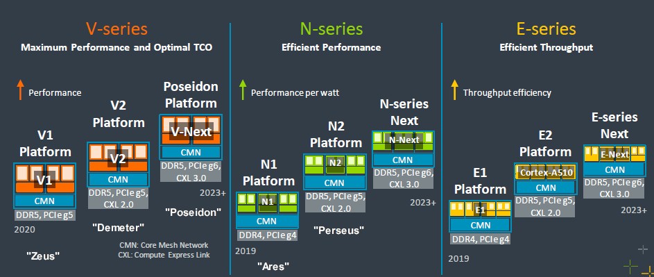
Originally, there was only one family of cores – the N series – but Arm trifurcated it into three families of cores and three corresponding platforms, each aimed at different parts of the systems market. The N series cores and platforms were aimed at mainstream server workloads where performance per watt drove the design, while the V series had heavier vector processing and were aimed at more compute intensive workloads such as AI training and inference and HPC simulation and modeling. The E series were aimed at throughput computing and optimized not just for higher performance per watt, but the most throughput in an even lower thermal envelope than the N series could deliver. Now there will not only be three families of cores and platforms, but two approaches: The DIY and the CSS, as it were.
So now the new Neoverse roadmap looks like with the CSS option shoehorned into it:
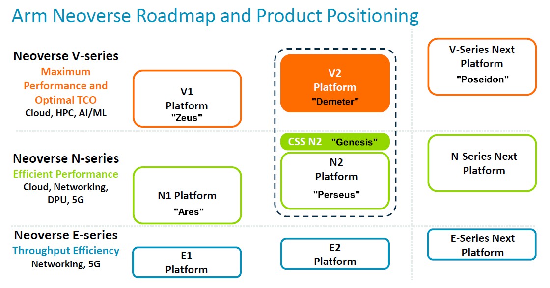
We have added the code-names for each core and platform where we know them.
The Neoverse effort allowed chip companies to get a leg up on their designs, and many have. Fujitsu started way earlier than any of the current vendors – years before there was a Neoverse effort – with its A64FX chip and could be considered the “Kronos” V0 implementation in many respects, since it invented the Scalable Vector Extensions and took it to the 512-bit vector extreme of the Intel AVX-512. Amazon used the “Maya” Cortex A72 in the original Neoverse stack in its Graviton1 chip, the “Ares” N1 in its Graviton2 chip, and the “Zeus” V1 in its Graviton3 chip. Nvidia originally used its Arm architecture license to create its “Denver” server processors more than a decade ago, but has switched to the V2 cores for the “Grace” CPU chips that are coming to market now. Ampere Computing had N1 cores in its Altra and Altra Max Arm CPUs, but is now doing custom cores. Alibaba has done a custom Arm v9 core, apparently, for its Yitian 710 processor, and if that is true, then Nvidia’s Grace does not have the first Arm v9 cores on the market. The Indian government is using the V1 cores in its “Aum” A48Z processor.
There are others, but these are the biggies. And they have all spent a lot of money creating their Arm server chips. But this is as much about time as it is money. And as we all know, Einstein proved that time is money gone wild as well as proving energy is matter gone wild.
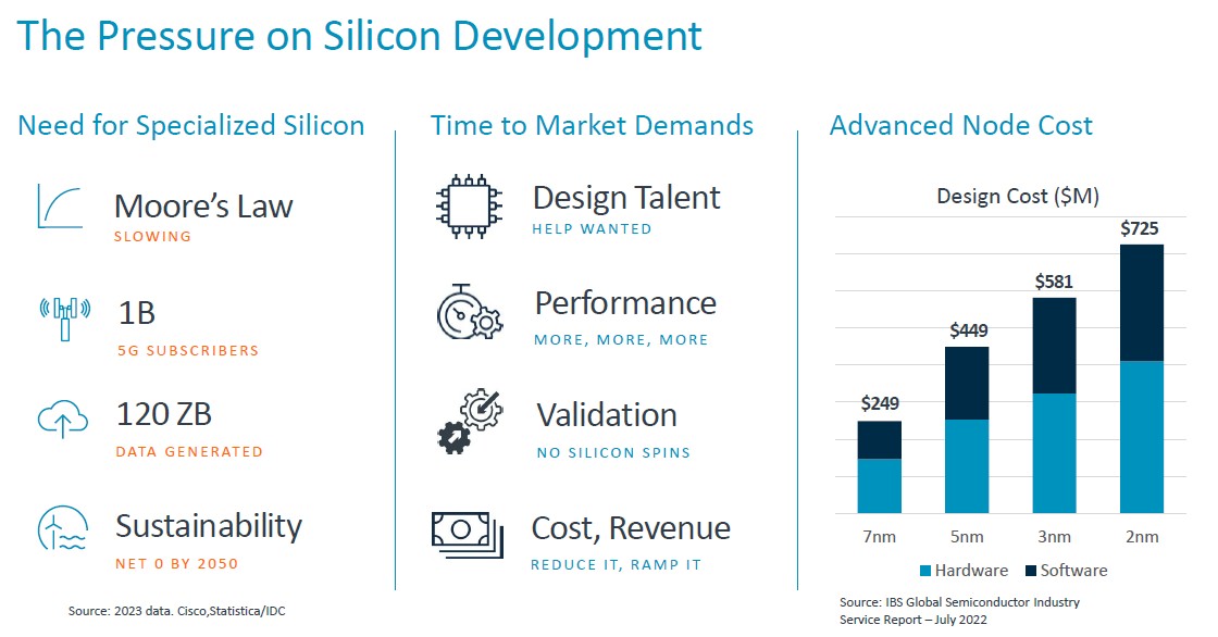
The pressures on chip designers, as Jeff Defilippi, senior director of product management at Arm, explained ahead of the Arm presentations at Hot Chips, are mounting just as the need for specialized silicon is growing as Moore’s Law runs out of gas. The cost for designing chips is rising as the transistor dimensions are sinking, as the chart above shows, and the cost per transistor manufactured is rising after the 7 nanometer node, which this chart does not show.
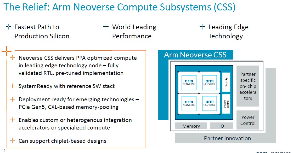
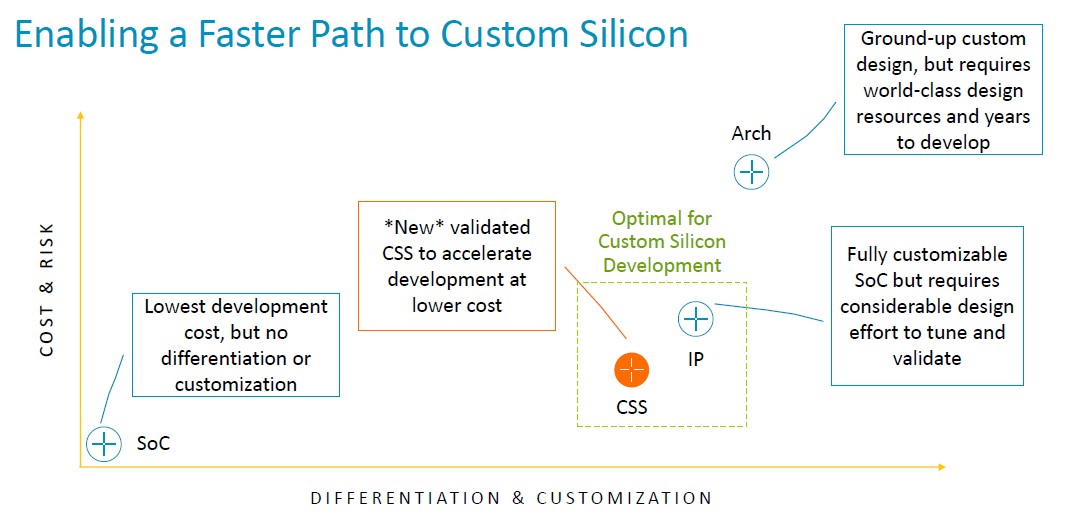
The CSS intellectual property package from Arm aims to speed up designs and, in the sense that time is money, at least convert money back into time saved, which again as Einstein proved, is money saved and money gained through earlier sales. (We presume CSS costs more than regular IP licenses because it includes more, but the risk is a lot lower and that the product – not the sum, but the product because these are multiplicative effects not cumulative ones – of cost and risk is therefore lower.)
Here is where the CSS package looks like conceptually:
And here is how it compares to licensing an SoC, an IP license, and an architectural license:
“Essentially the product is a multicore design that Arm stitches together,” Defilippi explained. “So this is the interconnect, the CPUs, the virtualization IP requirements – we stitch that together, validate it, and deliver it as a production-ready RTL deliverable to our customer. In addition to the RTL, we provide extra goodies associated with it: We provide an implementation package, the floor plan, the implementation scripts, and the physical IP libraries that are needed to hit that performance and the power envelope that’s required for their design on leading edge technology. We provide a complete software reference stack. So this includes everything from firmware, power management, management of the system, runtime security that’s required for the system. And we provide that reference stack to make sure that that software development starts on day one, and our customers have a nice starting point to begin with. And last but not least, we include our leading edge technologies beyond just the process node. Every year, there’s something new and exciting coming out. And certainly an example of that right now is CXL memory expansion pooling.”
Now imagine, particularly if you are in China, India, Africa or even at a cost-conscious hyperscaler, cloud builder, or HPC center in the United States or Europe and you do not have a deep pool of skilled engineers familiar with advanced server CPU design or the tools to design and test them properly to get a next-generation chip out the door fast. Then a CSS approach might not only speed things up considerably, but make it possible for a chip to be made in the first place.
But the time matters, and here is how Arm calculates the time saved via the CSS package compared to using a plain vanilla IP license:
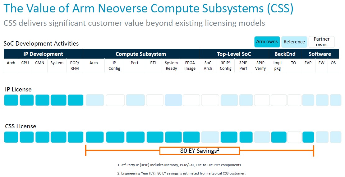
A savings of 80 engineer-years is pretty significant, particularly when there are still degrees of freedom for customization.
The questions are this: How valuable is a CSS design compared to one where the chip maker has done a lot of work? How much does it cost to get a chip from concept into a server or network device or storage array, and how much cheaper is that than using an X86 server from Intel or AMD or an Arm chip from Ampere Computing? Will any of this it be worth the trouble?
Well, with AWS and Alibaba making their own Arm chips, and Google rumored to be doing so, and Microsoft, Tencent and Baidu (along with Alibaba, Google, and Oracle) using Ampere Computing’s Altra Arm chips, it seems like it is worth the trouble. The Arm CPUs save them money and are representing an increasingly large part of their server fleets. And, they have more direct control through their own efforts and more indirect control through tight partnerships with Ampere Computing.
The hyperscalers and cloud builders will still buy lots of Intel and AMD CPUs, of course. But as we have said many times, that will be to support legacy Windows Server and sometimes Linux applications, and they will intentionally charge a premium for instances based on them – as will Intel and AMD for the underlying chips. No one is colluding on the tiering we see, but Intel and AMD have no incentive to compete with Graviton and the rest. They just cede that 15 percent then 20 percent then 25 percent of the hyperscale and cloud fleet to Arm and they are happy with the 85 percent then 80 percent and then 75 percent of a larger fleet that they can get without going into a price war.
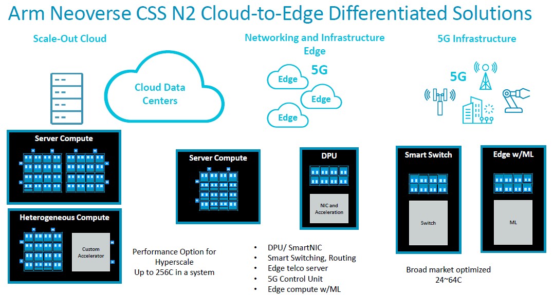
The CSS implementation of the “Perseus” N2 core meshes scale from 24 to 64 cores, and four of these can be ganged up in a package to scale to 256 cores in a socket using UCI-Express (not CCIX) or proprietary interconnects between the chiplets as customers desire.
Given the expected HPC and AI vector math that many of modern processors will be doing, it is a shame that there is not a CSS for the V2 designs. Perhaps that will happen – we strongly encourage that, and certainly by the future V3 designs some years hence. For now, Arm is starting the CSS effort only with the N2 designs, right in the middle of the roadmap.
Now, brace yourself for some beautiful schematics and block diagrams on the Genesis CSS N2 package, which were presented by Anitha Kona, an Arm Fellow and a lead system architect at the chip IP designer.
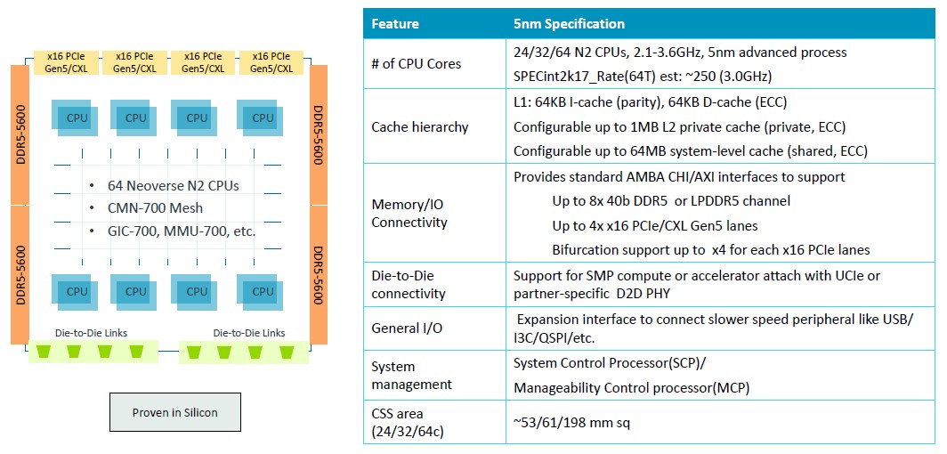
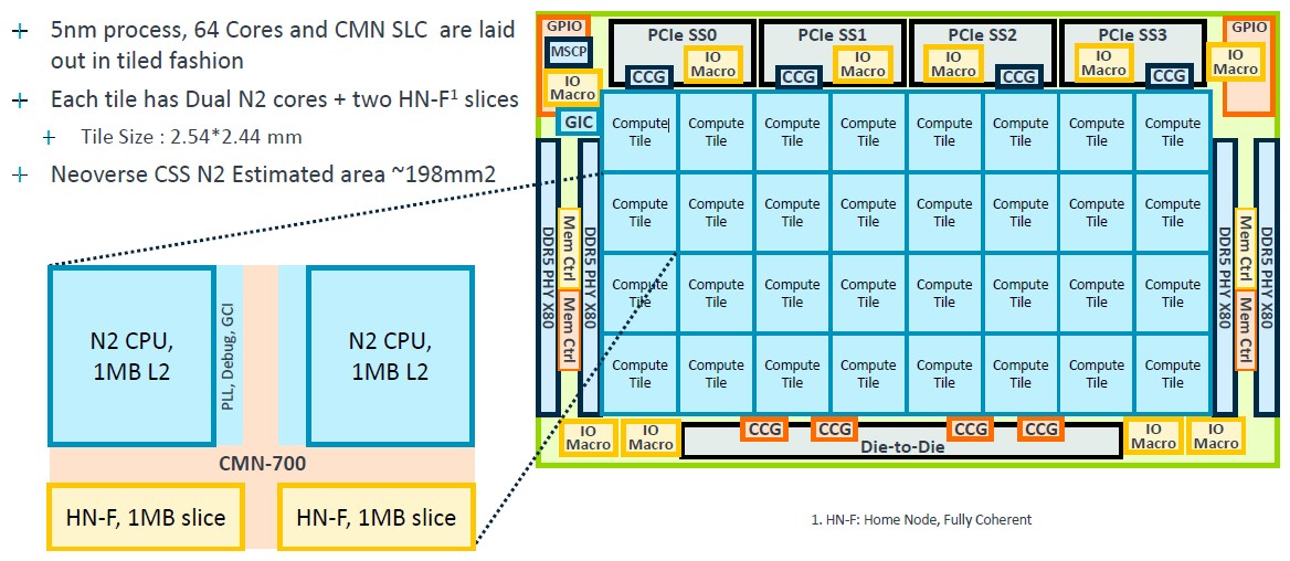
Here is the 64-core base block in the Genesis package at 5 nanometers from TSMC:
This is what the block diagram looks like:
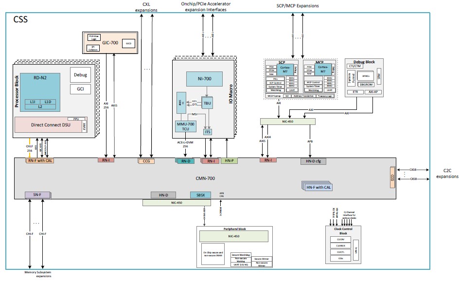
The CSS N2 package is SystemReady compliant to Arm Base System Architecture 1.0, Arm Server Base System Architecture 6.1, and Arm Server Base Boot Requirements 1.2.
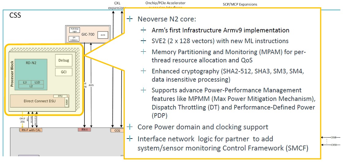
The N2 core is Arm’s first Armv9 implementation, but the V2 core could not have been that far behind with Grace now in the field and as far as we know, Nvidia got the V2 core finished from Arm. There is a chance that Nvidia and Arm collaborated on the V2 core design, much as Fujitsu and Arm did on what we have called the V0 core with our tongue firmly in cheek. Here’s what the processor block looks like for the N2 core:
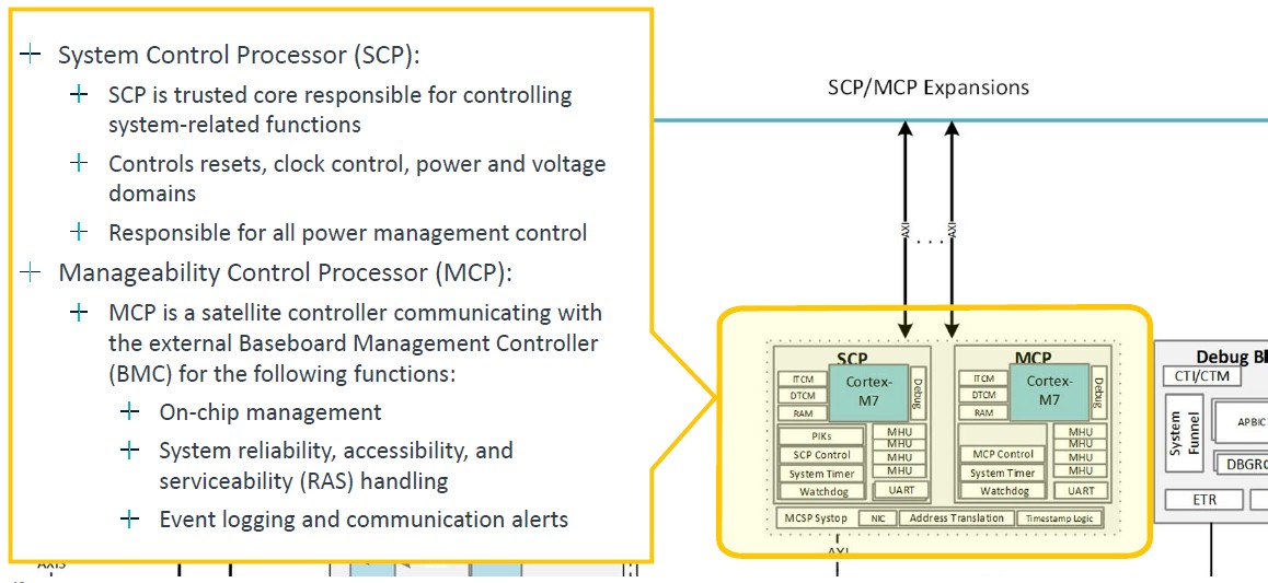
Two SVE2 128-bit vectors is not so bad, but the V2 has four of them. Which is where there needs to be a CSS V2 offering, hopefully not code-named “Exodus,” soon. Like, er, right now. Anyway, here’s the system control and management drill down:
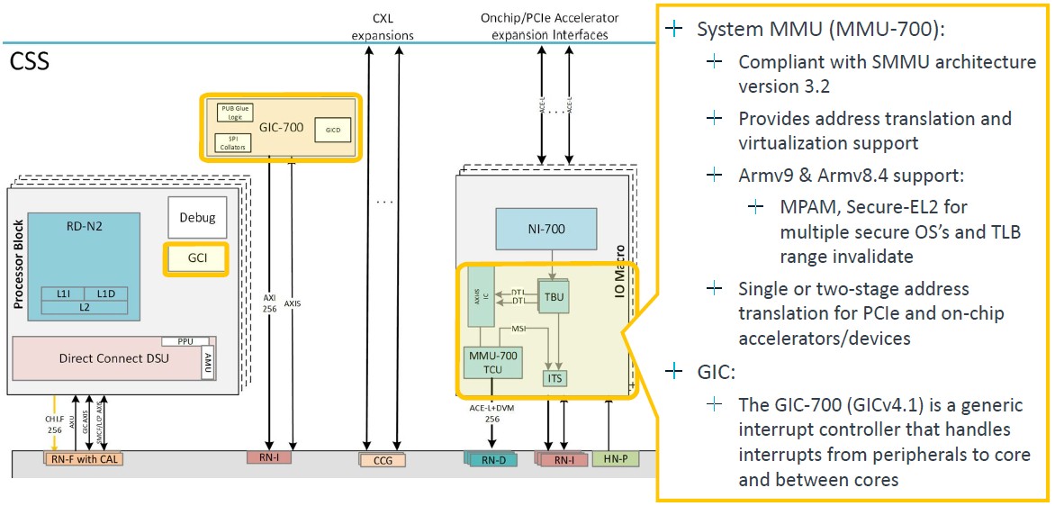
The zoom on the system memory management unit and interrupt controller is thus:
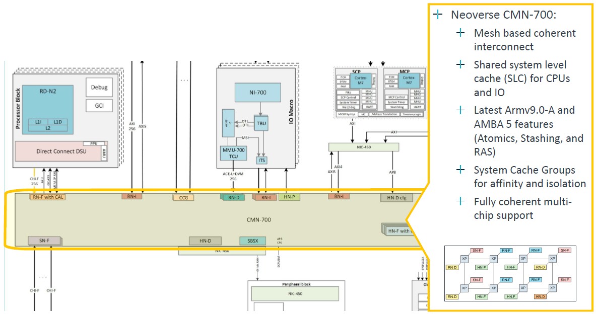
The core blocks are lashed to each other using the CMN-700 mesh, which has been around for a few years, which has been tweaked for the Armv9 designs, and which runs at 2 GHz:
The Genesis package includes a floorplan for an N2 CPU, which can be scaled from 24 cores up to 64 cores, and the 64-core floor plan looks like this:
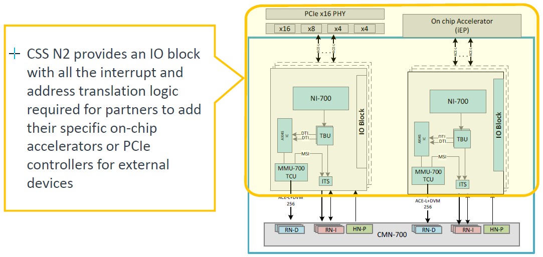
The CSS N2 package also includes an accelerator attach block that allows for the snapping in of PCI-Express and therefore CXL controllers:
There are interconnects that allow for two of four of the 64-core N2 blocks to be linked to each other. A Pair of chips make use of a chip-to-chip PHY that implements a straight symmetric multiprocessing (SMP) link and CXL PHYs are used to cross-couple a pair of these pairs to create a four-way package with 256 cores, like this:
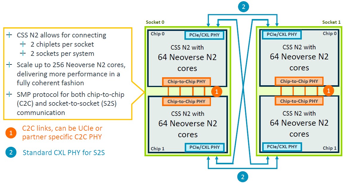
And here is the further zoom on how those SMP connections work:
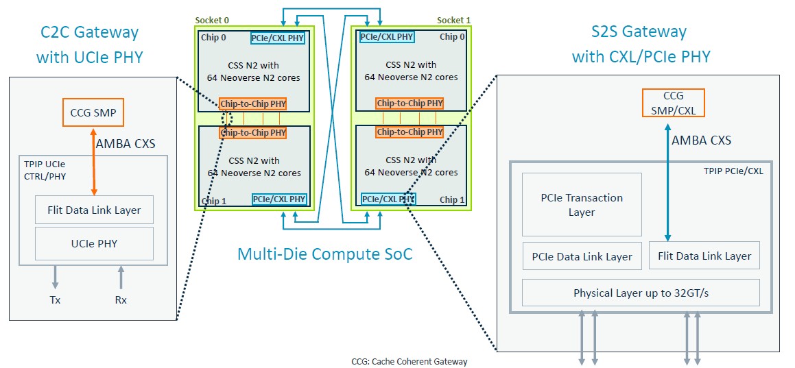
The PCI-Express/CXL blocks obviously allow for CXL Type 3 memory expansion above and beyond whatever memory controllers are embedded on the mesh interconnect. (It would be very helpful if the memory controllers and Ethernet controllers were part of the Genesis package.)
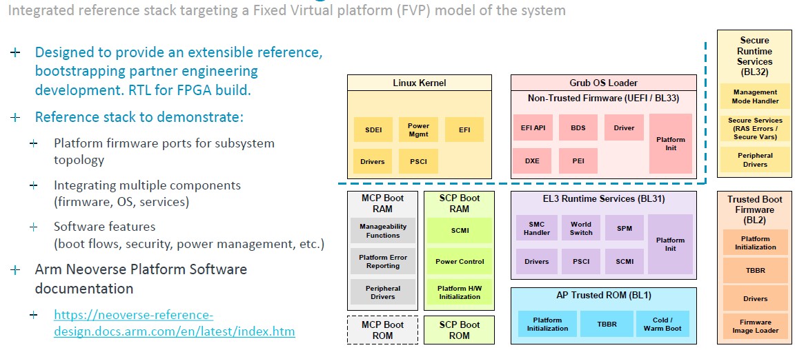
And finally, here is the software that is part of the Generis package:
Add it all up, and Kona says that Genesis IP package licensees can grab the CSS N2 stack, differentiate on memory, I/O, accelerators, and physical topology and go from kick-off to working silicon in an amazing 13 months and save that 80 engineering-years of development effort. Those are two stats from two different Arm partners who were early adopters of Genesis, so be careful about mixing those data bits into one promise. But clearly, both time and money – which is also time – can be saved in Arm CPU chip design.
We look forward to seeing V series and E series equivalents to the CSS N2 package.

Chip Roadmaps Unfold, Crisscrossing And Interconnecting, At AMD
After its acquisitions of ATI in 2006 and the maturation of its discrete GPUs with the Instinct line from the past few years and the acquisitions of Xilinx and Pensando here in 2022, AMD is not just a second source of X86 processors. Now, without question, it is a formidable …
Cloud Foundation Updates Reflect The New VMware By Broadcom
Broadcom’s $69 billion acquisition of virtualization stalwart VMware was not an easy proposition. Regulators around the world worried about the effect the deal would have on the IT industry and Broadcom had to make some promises – such as to the European Union, which demanded concessions from the semiconductor giant …

Server And Storage Spending Growth Looks Rosy Out To 2027
For a market that is so integral to the global economy, it sure is hard to get a complete dataset on quarterly and annual spending on information technology. We try to gather up all of the information we can find and flesh it out where we can so you can …
Even with a brain like that of Albert Franklin (a penny saved is a time earned), or Benjamin Einstein (matter gone wild energizes money, and house-keys hooked-up to kite-strings), it will be hard to differentiate between Cascading-Style-Sheets, Cross-Site-Scripting, Complémentaire-Santé-Solidaire, and this latest CSS offering from ARM. Could NCS (Neoverse-Compute-Subsystems), or even ACCS (ARM Complete Compute Subsystem), have been a better acronym?
CHARM could be a Complete Hyperscale environment for ARM (as it also involves bring-up and driver software).
HICUPS would be the Holistic Integration of Computationally Unified Parts and Subsystems (digestively yours).
This mARMite of possibilities is Genesis for virtually endless verses of tech neologisms (neoverses?)!
Exactly!
Given the lawsuit with Qualcomm and Nuvia, it seems plausible ARM wants those architectural licenses to go away. Could CSS be more profitable because one can customize the same product multiple times, sort of like PeopleSoft does with Oracle?
At this point the quality of LLVM and the GCC open-source compilers along with the fact that almost no application software is written in assembler means that “starting with a custom ISA” is actually not a massive porting job. How quickly RISC-V had a full Linux distribution–not to mention Loongson–are two examples. Even back in 1995 Linux ported quickly to the DEC Alpha and Sun SPARC.
The difference today is that Linux has become the industry standard for AI, high-performance computing, cloud and on-premise data center. Thus, a new computing architecture is immediately practical once Linux runs.
Well said, and good points.
I have 2 rejoinders.
1. Sierra Forest: https://www.servethehome.com/intel-xeon-e-cores-for-next-gen-sierra-forest-and-more-at-hot-chips-2023/
2. SiFive (and friends):https://www.servethehome.com/ventana-veyron-v1-risc-v-data-center-processor-hot-chips-2023/ plus https://www.servethehome.com/sifive-p870-risc-v-processor-at-hot-chips-2023/
Homegrown stuff like Graviton will continue obviously and then there is Nvidia’s Grace Hopper. But Ampere pulling stuff like this https://www.phoronix.com/news/Ampere-Computing-Steam-Play makes me very skeptical about it reaching the 25% thing.
I’ll get to my coverage on these. But I love Patrick, as he well knows.
These RISC-V folks are doing great design work for performance! With data center as a target, they should really publish results of SPECjvm and/or SPECjbb — SPECint2017 is not quite representative of those workloads …