
We have been waiting for years to see the first discrete Xe GPU from Intel that is aimed at the datacenter, and as it turns out, the first one is not the heavy compute engine we have been anticipating, but rather a souped up version of the Iris Xe LP and Iris Max Xe LP graphics cards that were launched at the end of October, which themselves are essentially the GPU extracted from the hybrid CPU-GPU “Tiger Lake” Core i9 processors for PC clients.
In this case, the Xe LP Server GPU, as this datacenter variant is called, is not aimed at HPC or AI compute acceleration, but rather at the video transcoding, cloud gaming, and cloud rendering workloads that Intel has historically supported with its “Skylake” Xeon E3-1500 v5 processors launched in 2016 or with its more recent “Coffee Lake” Xeon E-2100 processors launched in 2018. There was a Coffee Lake Refresh variant, called the Xeon E-2200, that came out in 2019 as well. These processors and their Xeon E3 predecessors have a modest CPU and a modest GPU – at least by datacenter standards – on a single die, and while we have argued in the past that they provide the cheapest flops available at the time on those integrated GPUs (it only adds a few ten bucks at end user pricing and a few watts of power to activate that GPU capacity) from Intel. As far as we know, there is not a Xeon E-2300 based on current “Tiger Lake” Core i9 processors in the works, but clearly Intel could do that.
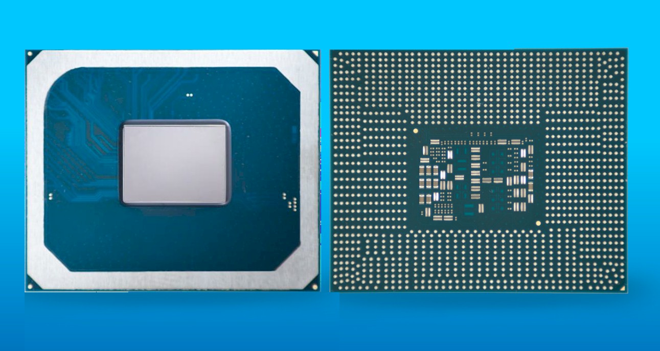
Instead, what Intel has done is busted out that integrated GPU from the Tiger Lake hybrid CPU-GPU processor, goosed it with more capacity, and packaged it up so it can be used as a discrete graphics or compute device in any client or any server. This discrete GPU is also known as “DG1” and “SG1” inside of Intel and is known as the Iris Max Xe LP GPU when sold for clients and now the Intel Server GPU when it is packaged up for server form factors. (Presumably, the D in DG1 is for desktop and the S in SG1 is meant to denote server.) This DG1/SG1 discrete GPU and the Tiger Lake processor that has a variant of it integrated on the die are all etched using Intel’s 10 nanometer SuperFin process.
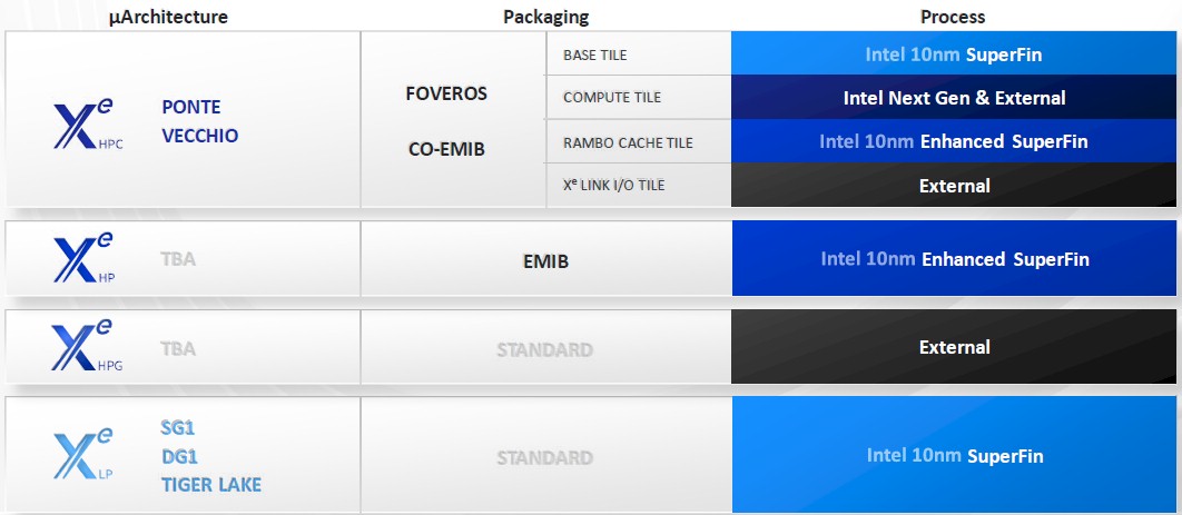
And if you are trying to keep the naming conventions straight, these DG1 desktop and SG1 server implementations are not the Xe HPG device, code-named DG2, that is going to be aimed at higher end gaming workloads. This DG2 device sits below the Xe HP device, which will be aimed at “enthusiasts,” whatever that means, and well below the “Ponte Vecchio” Xe HPC device that will be at the heart of the future “Aurora” A21 supercomputer. You will recall that Intel talked a bit about the Ponte Vecchio Xe HPC GPU and its “Sapphire Rapids” Xeon SP processor companion at SC19 last year. With Intel’s recently slip with its 7 nanometer process, Ponte Vecchio is now shipping in late 2021 or early 2022. The Aurora nodes have six Ponte Vecchio GPUs lashed to a pair of Sapphire Rapids Xeon SPs, with what we presume are PCI-Express/CXL interconnects between the CPUs and the GPUs to present a unified memory.
What is obvious from the table above is that Intel has been hedging its bets on components in the Ponte Vecchio device, using a chiplet design with Foveros 3D stacking and Co-EMIB 2.5D interconnects between chiplets. The base Ponte Vecchio tile and the cache tiles for this discrete GPU are being etched in the 10 nanometer SuperFin processes, the compute tiles are either going to be 7 nanometer Intel processes or those from another foundry – there are only two choices, and they are Taiwan Semiconductor Manufacturing Corp and Samsung Electronics – while the Xe Link I/O tile for the discrete GPU is being etched externally. We have no idea what process that is using or what foundry, but if it was 14 nanometers then Intel would use its own well-matured process and not GlobalFoundries. It is odd that this is being done externally at all, really.
In any event, the Intel Server GPU is not that device, which is sad for us as we enter the SC20 supercomputing conference. At the moment, the Intel Server GPU is shipping in an early stage preview to H3C Technologies, the partnership in China between Hewlett Packard Enterprise and Tsinghua Unisplendour, Lynn Comp, vice president of the Data Platforms Group at Intel and general manager of its Visual Infrastructure and NPG Strategy division, tells The Next Platform. One of the early adopters is Tencent, which owns a 48.4 percent stake in Epic Games and which has its own aspirations in online gaming.
There are not a lot of technical details on the Intel Server GPU, except that it has a 128-bit wide pipeline and that it has 8 GB of LP-DDR4 memory integrated on it.
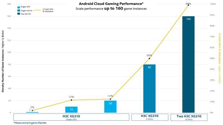
The H3C XG310 PCI-Express card shown in the feature image at the top of this story puts four of these devices and links them to a server node over a PCI-Express 4.0 x16 slot. We have no idea how many PCI-Express lanes come off the DG1/SG1 chips, and Intel is really not providing much in the way of detail on this GPU. It is not clear if the GPUs are crosslinked in some fashion using the Deep Link load balancing protocol, which allows a CPU to be equipped with multiple Iris Max GPUs and spread work across them, in some fashion across these four GPUs. In fact, it is not clear at all how they are linked.
We have no feeds and speeds to speak of for the Intel Server GPU, but we do know that the Iris Max chip had 96 execution units (EUs) on its chip, it clocks at 1.65 GHz, has 4 GB of memory with 68 GB/sec of memory bandwidth, and supports DLBoost machine learning acceleration on its math units and can balance the processing of those instructions across the Xeon SP CPUs (if they support DLBoost, which is just a funky name for mixed precision vector math) and multiple Intel Server GPUs. We have no idea how much juice the Intel Server GPU burns, or how much it costs because Intel is not saying.
What Comp did tell us, however, is that a single card with four of these Intel Server GPUs can handle up to 80 Android game users with graphics running at 720 pixel resolution at 30 frames per second, and the rate could be doubled up to 160 users with a pair of cards in the server.
Below is how Intel stacks up the server card against Nvidia’s Tesla T4 accelerator for video transcoding, which is probably not a fair comparison with the new “Ampere” A40 and A6000 GPU accelerators, based on the GA102 and GA104 GPUs, respectively, out the door offering considerably better oomph.
![]()
Somewhat more detail is available on these benchmarks at this link.
The reason we are paying attention to the Intel Server GPU launch is because it is important for the chip maker to take on all workloads in the datacenter – not just HPC and AI – to make a business out of its discrete graphics chips and to realize its aspirations. The more bases it covers, the greater the TAM and the more intense the competition, which is good for datacenter operators.
But more importantly, we wonder if companies will want such modest devices when the bigger GPUs, which are more costly, can at least run more of the workloads that are in a modern datacenter. As we have pointed out before, general purpose computing is not something that is going away, but rather general purpose computing based only on the X86 processor is going away. There is no reason that an X86 processor paired with GPUs supporting a diversity of compute can’t be the new general purpose compute in the datacenter. And as such, hyperscalers and clouds that have lots of workloads and that do not want to create islands of compute – this bank of GPUs for video encoding or cloud gaming, this other bank of GPUs for machine learning inference and maybe certain kinds of HPC simulation and modeling, and that other bank of GPUs for HPC and machine learning training – might be more inclined to get volume pricing on a single high-end GPU and forego balkanizing their datacenter.
In that case, having a broad and diverse portfolio actually hurts Intel – or any other GPU maker – more than it helps them.
It will be interesting to see how this all plays out.


“No Quick Fixes” As Intel Losses And Restructurings Continue
Intel’s new chief executive officer, Lip-Bu Tan, has his work cut out for him, just like his predecessor, Pat Gelsinger, did several years ago. And given the even worse state that Intel is in – generating less cash on lower sales and therefore making it that much harder to raise …
Chip Roadmaps Unfold, Crisscrossing And Interconnecting, At AMD
After its acquisitions of ATI in 2006 and the maturation of its discrete GPUs with the Instinct line from the past few years and the acquisitions of Xilinx and Pensando here in 2022, AMD is not just a second source of X86 processors. Now, without question, it is a formidable …
It’s All Uphill From Here For Intel’s Datacenter Business
Intel’s Data Center Group has just turned in the third best revenue quarter in its history, just behind the two thirteen-week periods that started off 2020, which was before the coronavirus pandemic had hit and just after it hit and the full effects were not seen as yet. Oh, and …
The Xe update yesterday also listed Xe-HP status as “Sampling”. The announcement also stated it is available on their devcloud.
I wonder whether Amdahl’s lawn is what makes this 4x baby-GPU configuration viable. Namely that speedup of solving large single problems is limited by sequential bottle-necks; so if there are enough concurrent problems (or separable sub-problems) an element of coarse-grained parallelism can increase system-level performance/$. That’s analogous to CPU application architectures which use SIMD and threading within each NUMA node, and MPI between NUMA nodes.