

AMD gets a lot of credit for creating Accelerated Processing Units that merge CPUs and GPUs on a single package or on a single die, but Intel also has a line of chips Core and Xeon processors that do the same thing for workstation and server workloads. The “Skylake-H” Xeon E3-1500 v5 chips that Intel recently announced with its new Iris Pro Graphics P580 GPUs pack quite a wallop. Enough in fact that for certain kinds of floating point math on hybrid workloads that system architects should probably give them consideration as they are building out clusters to do various kinds of processing.
We would be the first to admit that the Xeon E3 would be an unconventional choice for hybrid CPU-GPU workloads, much as was the case with AMD’s “Kyoto” X1150 and “Berlin” X2150 lines of Opteron X series APUs. But the relatively inexpensive and powerful GPUs are nonetheless compelling for those who are looking to cram a lot of nodes into a rack of servers that can do a mix of single-threaded and floating point work and do so with very good bang for the buck.
The sales pitch from Intel about the Xeon E3-1500 v5 processors did not mention that the 72 GPU cores on the Skylake-H processor could be used for floating point math acceleration per se, but of course this GPU can be turned into an offload engine like any other GPU linked to a CPU. This, as far as The Next Platform is concerned, is where the Xeon E3-1500 v5 processors get interesting. The same hyperscale, service provider, and cloud builder organizations that might be looking at the Skylake-H processors to speed up video streaming or encoding workloads can also think about deploying the same infrastructure to do parallel floating point operations on the relative cheap.
The Skylake-H Xeon processors are implemented in the same 14 nanometer processes that Intel uses to etch its Broadwell Xeon E5 v4 and Xeon E7 v4 processors, which have both been recently announced. They feature the Skylake Xeon core, and give us a preview of sorts about what we can expect from next year’s Skylake Xeon E5 and E7 rollouts. We do not have the instruction per clock (IPC) ratings relative to the Broadwell cores at a constant clock, but we will expect to see that when Intel puts together the presentations for the Skylake Xeons next year. With Skylake being a “tock” in the tick-tock scheme Intel uses to advance its chips, the process stays the same but the microarchitecture gets improvements. From early tests of the desktop variants of Skylake cores, it looks like the IPC has gone up around 3 percent, but that may not hold for the server implementations and the number could be a bit higher. (We would expect something more on the order of 8 percent to 10 percent, given past history for microarchitecture improvements.)
While the performance of the CPU cores on the Xeon E3-1500 v5 processors is interesting for single-threaded applications, these four cores with eight threads do not provide all that much oomph. Was is intriguing is the fact that the new Iris Pro P580 graphics engine on the chip has 72 graphics cores, up from 48 graphics cores with the P555 engine used in the Broadwell Xeon E3 v4 hybrid chips. We asked Intel for the floating point ratings for the GPUs inside the Skylake-H chips, and it turns out the Iris Pro P580 delivers only 331.2 gigaflops at double precision running at its Turbo Boost speed of 1.15 GHz, but the single precision performance is a very respectable 1.32 teraflops. Yes, that is about 20 percent of the expected single precision performance of the “Knights Landing” Xeon Phi parallel processor, which has 72 active “Silvermont” Atom cores with a pair of 512-bit AVX 3.0 vector engines on each core. The Knights Landing chip is expected to deliver more than 3 teraflops at double precision and twice that at single precision, so it packs a punch to be sure. But for workloads that do not require low latency interconnect and that can fit their data and applications in the relatively small memory footprint of the Xeon E3 chip, this is clearly an option.
You can’t beat the price of the Skylake-H Xeon E3 chips, as the table below shows:
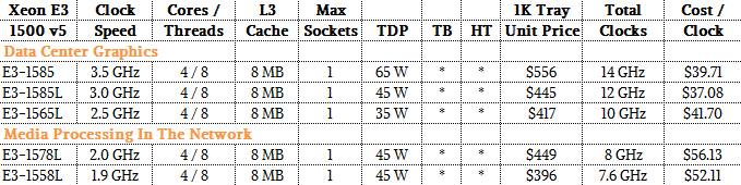
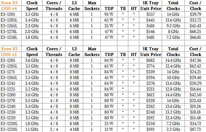
It is hard to reckon what the value of the integrated GPU is on these chips, but with the “Haswell” generation of chips, the top-end E3-1285 v3 chip cost $682 with the HD Graphics Pro P4700 GPU, which had 20 GPU engines, cost $682 each when bought in 1,000-unit trays, while the E3-1280 v3 with the GPU turned off cost $612. That GPU was rated at 412 gigaflops, which worked out to $170 per teraflops single precision. (This does not take into account the vector units available in the Skylake cores.) That is very cheap, obviously. Here is how the new Skylake Xeon E3 chips stack up to the prior generations of the Xeon E3s:
This GPU in the Skylake-H Xeon chip offers very compelling bang for the buck for single precision floating point math.
The latest “Pascal” GPU from Nvidia costs on the order of $10,500, as best as we can figure from Nvidia’s pricing on the DGX-1 hybrid server, and delivers 10.6 teraflops at single precision. (Pascal also delivers a huge amount of memory bandwidth and lots of other benefits, too, like NVLink clustering for GPUs.) That works out to $990 per teraflops. If a top-end Knights Landing Xeon Phi costs on the order of $4,500 for a 6 teraflops part, that works out to $750 per teraflops. All that we are saying is that the flops on that integrated Iris Pro P580 GPU that comes with the Xeon E3-1500 v5 could be on the order of $100 to $150 per teraflops, depending on how you want to allocate the value of the GPU (which we have to guess because Intel is not offering versions of the Xeon E3-1500 v5 without the GPU included).
We would love to see what happens when someone tries to build a cluster out of such chips, and not just to do video streaming and transcoding as Intel suggests is the target workload for these devices. It may be a bit tricky to get OpenCL to do the offload to these GPUs, but it can be done.

Finally: Some Good News For The Intel Xeon CPU Roadmap
It was a reasonable enough gut reaction given the many changes happening at Intel in recent months. The chip designer and maker – the last one in the world that does both – had announced a datacenter product line update for Wall Street analysts only a week after Raja Koduri, …
Berkeley Lab Opens Bidding For Future NERSC-10 Exascale System
The National Energy Research Scientific Computing Center at Lawrence Berkeley National Laboratory, one of the key facilities of the US Department of Energy that drives supercomputing innovation and that spends big bucks so at least a few vendors will design and build them, has opened up the bidding on its …

AMD Turns The Screws With “Turin” Server CPUs
If you are looking to upgrade your X86 server fleet – and there is lots of chatter about how many enterprises as well as hyperscalers and cloud builders are in the financial mood to do that – then the good news is that both Intel and AMD have now rolled …
And how would one program these GPU cores for compute? Does Intel support OpenCL for its onboard GPUs on Linux, which is what almost everyone building compute clusters uses?
I haven’t tried it myself in anger, but the January 2016 release of OpenCL SDK from Intel does support Skylake under Linux. I believe it’s opencl 1.2 with a preview of 2.0. I assume it’ll function correctly on the E3 based on Skylake, it’s essentially the same die as some of the non-Xeon models, but again, haven’t verified that myself.
Yes it does since a long time now, see first entry in the FAQ
https://software.intel.com/en-us/intel-opencl-support/faq
This is definitely fuzzy maths, where is the complete specifications on the integrated GPU, what are the EU counts, the ROP counts, etc. Why are the core clocks on the Intel CPU cores added cumulatively and what about the Flops/watt metric, given in gigaflops/watt or megaflops/watt. This cost/clock metric smacks of desperation from Intel, and what of Intel’s GPU/Graphics asynchronous-compute ability. The Pascal SKU is Nvidia’s highest priced kit, what about throwing in some of AMD firepro SKUs metrics into the mix also, or even Nvidia’s Maxwell generation Quadro SKUs for a better comparison. Nvidia has priced that GP100 silicon like Intel has priced its 10 core consumer E series SKU, way above its true computational value.
Furthermore where are the certificated pro drivers from Intel for that “graphics” to work with all of the pro CAD/graphics packages? We all know that much of the cost that goes into the pro graphics/workstation SKUs from Nvidia/AMD come from the costly driver certification process with the market’s main graphics/workstation packages, so where is Intel’s graphics drivers in the total equation, and after the sale graphics driver support? And finally, how do these CPU cores on Intel’s SKUs rate against any Power8s SKUs, and let’s include some third party OpenPower SKUs for the costs comparisons with Power8. Really Intel is grasping at straws here that cost/clock metric, and adding clocks up cumulatively for some sort of statistical obfuscation which with to compete with the GPUs that will put even the latest Xeon Phi to shame for that total FP flops metrics.
Nicely done on E3, iGPU and Perf/$. And possibly long overdue. The ‘Cost/Clock’ metric is a simple, yet effective in practice, starting point for comparisons. I have heard there are a few sites that have 10’s of thousands of E3 doing HPC, but that may just be rumor. My organization has experimented with integrated GPU for HPC. No luck thus far, but it does look promising.
Don’t forget that the Iris Pro P580 can also pump out 2.6 TFLOPS of fp16 floating point.
The programmability, conceptually, remains a great idea for those willing to demonstrate validations of that compute paradigm.
One question to consider is the software tools and validating developments effort worth the platform investment?
Broadwell E3 12xx v4 is absolutely rejected by the channel.
As of last week, E3 15xx represents 0.000368% of all Ivy, Haswell, Broadwell and Skylake generation Xeon broker inventories.
E3 15xx itself represents 0.330% of E3 12xx v5 stocks, 0.0774% of all Haswell E3 12xx v3 and 0.0241% of all Core Skylake generation broker channel inventories.
In other words secure your E3 15xx contract from Intel, first, for all development time, before proceeding.
Mike Bruzzone, Camp Marketing