

The chief technology officers in the tech world have done their time in the engineering trenches, writing their papers, getting their patents, and helping suppliers up and down the IT supply chain make the money that keeps the innovation flowing. But someone always needs to focus the imagination and enthusiasm of system architects, chip designers, and software engineers and design devices that solve real-world, actual customer problems.
At AMD, that someone is Mark Papermaster, who joined the CPU and GPU – and now DPU and FPGA – chip supplier in October 2011, three months before current president and chief executive officer, Lisa Su, was brought in to help transform the company. Papermaster was at IBM for 26 years, leading the development of many generations of System z and Power processors used in Big Blue’s enterprise-class and HPC systems; he then went on to work at Apple steering the development of its processors for iPods and iPhones.
We sit down to talk chip with Papermaster every now and again, and did so recently in the wake of the launch of the “Genoa” 4th generation Epyc server CPUs last month.
Timothy Prickett Morgan: When I spoke to your boss, Lisa Su, recently, one of the questions I asked her was about the pace of innovation that AMD could bring to bear with the Epyc CPU business. And she said that it would continue but did not have a lot of time to elaborate. But ultimately, as chief technology officer, you are the one who is actually on the spot to deliver, so I will ask you to elaborate. The last four generations of Epyc processors have had a certain pace of advancement, and it is accelerating, obviously, and the product line is broadening. Is that innovation pace is that sustainable over the next four generations?
I realize you can’t get into specifics, but for the longest time IPC improvements were maybe 5 percent to 10 percent per generation, and these days we are seeing 14 percent to 19 percent. The core counts are doubling and doubling and doubling. And there are other architectural and packaging technologies that are evolving fast. You got some clock speed increases this time around, which was neat, but generally clock speeds are inching down over the past decade and a half.
Can your chip architects keep pulling the rabbit out of the hat for the next four generations and the next five or so years of Epyc CPUs?
Mark Papermaster: It’s a great question. Here is how we think about it. With every generation we pull the best levers as far as we can to to progress real life workload performance for our customers. And so every generation, we look at what is available to us.
With the “Genoa” generation using the Zen 4, we were able to really go beyond the normal increase that we have with what I will call the “generation plus one” once we’ve done a new microarchitecture. So “Milan” had a brand new Zen 3 microarchitecture, and it was very well received and had leadership performance. We did a lot of fundamental changes in the pipeline to really widen it out. And it was still in 7 nanometer, which the previous “Rome” generation and Zen 2 had been in. But we did we still improve the performance per wat with Zen 3 and our Milan configuration that maxxed to 64 cores.
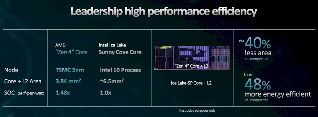
With the Genoa generation, we went above the normal that we would have on occasion. So I was extremely pleased with what the team was able to do thanks to the deep partnership we have with TSMC. We really leveraged 5 nanometer, and it really brought excellent power efficiency. But we also manage the overall chip capacitance, so the design elements are very, very finely tuned in some sense for Zen 3 and certainly for Zen 4 for server applications. You know, there’s also a lot of power in the areas outside of the Zen 4 core, in the I/O and memory die, which is in the center of our configuration. We took that from 12 nanometers with Milan to 6 nanometers with Genoa.
TPM: I was a little surprised by the magnitude of the I/O and memory die shrink. People keep telling me that it is really hard to shrink the I/O and memory chiplets because of the fact that they are driving signals and it is relatively easy to shrink the cores because they are just bit flipping. Sometimes when you shrink the I/O dies, the performance gets worse and the signal gets noisier.
Mark Papermaster: You are 100 percent right.
TPM: And neither TSMC nor Intel had a 10 nanometer process that was worth much, so I can see you having to go to 7 nanometers, but then you pushed it to 6 nanometers.
Mark Papermaster: You got it. So for two Epyc generations, we kept the I/O die at 14 nanometers and at with the third we shrank it to 12 nanometers. But eventually what happens is that the technology matures, and the analog mixed signal efficiency is there, and, frankly, the cost goes down. So you get the performance, power, and cost to bring that technology over and drive ROI.
But as you know, that gets harder as you go forward because those memory elements and analog mixed signals are still not scaling to the degree they are scaling with logic circuits. So you will continue to see us leverage technology to move chiplets at the optimum pace. This is how it came together for the fourth generation, and it really all came together.
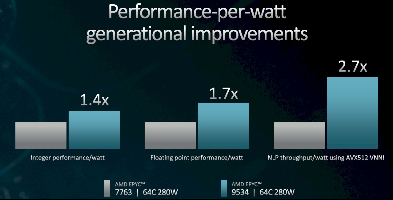
In this case, we had 5 nanometer process and design enhancements for the cores and with the I/O die we had a big technology change and the design optimization, too. From a performance per watt point of view, it is just a huge story. The specs I showed off at the launch tell the story: 1.4X on integer performance per watt, 1.7x on floating point performance per watt. And with AVX-512 support running BERT AI inferencing, we had 2.7X improvement generation to generation.
TPM: These are big jumps, core for core. You can’t do this every time, right?
Mark Papermaster: We are opportunistic, and at every transition, we’re going to pull every lever we can. And it’s not going to be consistent gen to gen. You’re just going to see different gains every gen. What our customers should do is look at the trend line and take an average on the dots and know that we’re going to be very aggressive gen over gen, always driving a gain in performance. Sometimes it’s a bigger IPC. Other times, it won’t be the IPC, it’ll be what we’re doing on throughput and overall total cost per core. So what we will do every generation is leverage the tools available, get the maximum customer benefit, and deliver it to them for what they care about.
TPM: I was born the same month Gordon Moore wrote his famous paper about transistor costs, and we have been thinking about the curves for transistor costs and densities literally as long as I have been alive. Which is neat. But Moore’s Law is really about cost of transistors driving density and that driving compute, it is not about driving density for its own sake. I would say that density and throughput increases are byproducts of lowering the cost.
If the costs have flattened out and in some cases are going up, what do we do in a world where transistor costs – including design and manufacturing and yield – keep going up even as densities increase with 3 nanometer, 2 nanometer, 1.8 nanometer and so on? Are we going to depend – and I might say overdepend – on ever-better 2.5D and 3D packaging techniques and the use of chiplets to make up the difference so the performance of a socket goes up faster than its cost of manufacturing?
Mark Papermaster: Let me back up because you had a lot in there. I will make a few comments.
First of all, I said even in my comments at the 4th Gen Epyc launch in November, the key for us in maintaining a Moore’s Law pace is our chiplet approach. We believe that chiplets have been highly instrumental on keeping us on an accelerated performance growth, despite Moore’s Law. And the cost per transistor is going up. The cost piece of Moore’s Law is gone. You can’t stay in the same cost window while doubling the density of a chip every 18 to 24 months – that part is gone. But the exponential need for more density and performance at those generational paces, that’s actually still the same. So how do you do it?
So there is a new Moore’s law says you have to leverage a chiplet approach. And we were delighted when we first went out with chiplets when “Naples” was our first server launch. People realize that that is the right way to go, and you do this by effectively putting the circuits on the process node they want to be on. This is a big jump for Genoa. The CPU core went to 5 nanometer from 7 nanometer, but as I said, the I/O die went from 12 nanometer to 6 nanometer – and because it was the right time for both. The cost/performance trade off was there. But on the leading edge node, the cost per transistor is going up at each new leading edge because the jump itself is more costly and the mask counts keep going up at every turn. It’s an expensive value proposition.
TPM: How much does the process cost go up every time? Is it 5 percent? More? Less?
Mark Papermaster: I won’t give you a specific percentage there. But I have said publicly is gone is the day when you can increase the density such that your cost per transistor is flat – it is going up. And so what we do is we are leveraging process waves and making sure that we are really bringing the performance to stay on at a Moore’s Law pace. So what that does is it puts more pressure on the designers to not only bring IPC on the CPU engine, but it’s going to drive us to more and more heterogeneous computing and leveraging other accelerators. That’s how we’re going to stay at pace.
And how do you put all that together? It does require more packaging technology. And the trick is to keep that package technology highly yielding. And that’s what we are very focused on. So what we do is make sure we’re not using esoteric packaging.
If you look at the 4th Gen Epyc that we have today, it’s the same organic substrate that we had in Epyc generations one, two, and three. We have taken advantage of the manufacturing learnings over that time, but it’s not an esoteric technology. Yet, where you need other capabilities – take 3D V-Cache as an example – that uses a hybrid bonding technique and that does add cost and cycle time. But again, it’s not esoteric. We are an early pioneer with hybrid bonding, but we didn’t jump over to it until it was established and with good manufacturing yields.
So, it really is about the design choices, the power optimization choices, the foundry node choices, and the packaging choices that you make. And you have to make very, very careful tradeoffs between these when you do each generation.
You can stay on the Moore’s law curve of performance and density, but not the Moore’s law curve of cost per transistor.
TPM: And the cost per unit of work is still going down, and that’s the good news because that is what drives both datacenter compute, personal compute, and consumer electronics.
Mark Papermaster: It is, and the power per unit of work is also going down. That’s what I’m so impressed with about our general CPU lines: the rate of change of kilowatts per unit of work.
TPM: But the thermals are still increasing as the logic density keeps going up even as the process shrinks are happening.
Mark Papermaster: It’s a very important qualification.
TPM: I think a lot of machinery in the datacenter will have some form of liquid cooling, in the chassis at the very least, because of this. Which is coming full circle back to the water-cooled thermal conduction modules, or TCMs, that IBM built back in the day with its System/3081 mainframes in the 1980s – until Big Blue switched from bipolar to CMOS processes in the 1990s with mainframe engines.
Mark Papermaster: As you know, I’ve been there and have literally done that. I was at IBM at the time and we would sit the chip on what we called the pogo sticks.
TPM: Like back then with bipolar chips, we are going back to this world where you are going to need to get all the wires close together, and that means you can only go up, and you are going to have this dense block that needs to be cooled.
Mark Papermaster: We can go up, but the pitch is coming down dramatically, both laterally and vertically. We do have thermal issues – you’re right – but you have thermal density. So when I talked about all the tradeoffs, you can add thermal management to the list I rattled off. All of this makes the architect’s job harder. But guess what? We have these new levers available to us. And at AMD, we’re really focused on using them in a smart way and making the proper tradeoffs to benefit our customers, gen over gen.
TPM: Do you do the packaging and cooling? Do you create this expertise internally? Do you license things? Do you do fundamental research by yourself and also with the foundries?
Mark Papermaster: We have phenomenal expertise and packaging at AMD that got even much stronger yet again with the Xilinx acquisition because Xilinx was doing chiplets long before the acquisition. So, you know, it’s been a great partnership. And the way that we do it is deep partnerships with the foundries and the offshore test and assembly houses.
Let’s take hybrid bonding as an example. This is innovation from AMD paired with innovations from TSMC. And it results in a leading edge capability that goes out to the whole industry. We pioneer it, so we get early access, because we innovated with them. But we want to we want to see the cost come down. So we’re happy for it to be available to the industry. That’s the whole foundry model, right? An economy of scale. This is a beautiful aspect of our semiconductor ecosystem. It’s a global ecosystem and it works amazingly well to bring innovations into mass manufacturing.
TPM: Where did the organic substrate the technology that you use to create all those generations of Epycs come from?
Mark Papermaster: That’s an older technology, and we have been using that organic substrate technology and honing it for years.
The newer technologies are all in 2.5D and 3D that allow us to then get broader integration with a tighter pitch, which you need for heterogeneous computing. You need it for GPUs. So if a GPU has super high bandwidth connectivity to its high bandwidth memories, that needs 2.5D , which we have pioneered with GPUs with HBM since 2015.
But then look at what we’re doing with the Instinct MI250, is called elevated fan out bridge. So it’s a very, very effective lateral conductivity. In the future, you can combine that type of lateral conductivity with the hybrid bonding we did with the vertical cache, and this allows us to get much more effective heterogeneous computing – CPUs with the accelerators. But it does come at the cost of a longer cycle time, and certainly higher packaging costs than what we’ve had in our organic substrates. So you have to use it very judiciously.
The architecture team has to make sure that it delivers the end customer value that in turn drives the pricing. So it’s all about architecting for end customer value.


As soon as materials fabrication gets back to all solid state on logic for long time, and with memory solid state inevitable, that can co-exist with radio on the same die, maybe not, everything will be fine. Photonics is interesting because it scales with solid state and its analog. mb