
The lines between the CPU, its main memory, the memory of accelerators, and various external storage class memories have been blurring for years, and the smudging and smearing is no more pronounced than with IBM’s Power9 family of server processors. This is a good thing and it is absolutely intentional.
The funny thing is that this blurring is happening at exactly the same time that there is a move to disaggregate the components of a system and make them more composable, and the irony might be that IBM could actually deliver on composability far ahead of its competitors, who are by and large bound to the Xeon processor but these days are also looking at CPU alternatives from IBM, AMD, or the Arm collective or at offloading to GPUs from Nvidia or AMD or FPGAs from Xilinx and Intel.
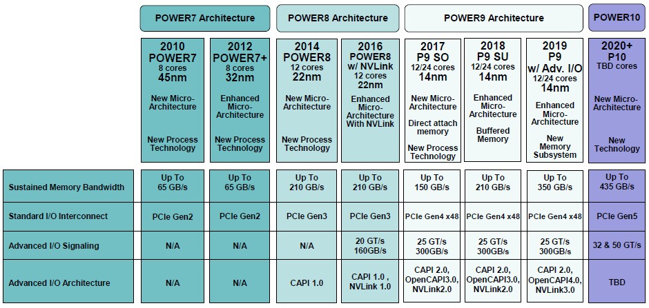
At the Hot Chips conference in Silicon Valley two years ago, Jeff Stuecheli, Power Systems hardware architect at IBM, divulged the salient characteristics of the “Nimbus” and “Cumulus” variants of the Power9 processors, which IBM started shipping this year. Back then, Stuecheli concentrated more on the Nimbus version of the Power9 chip, a 24-core processor with four threads per core that is aimed at workhorse two-socket machines and is specifically targeting the “Skylake” Xeon SP Gold and Platinum processors that do a lot of heavy lifting in the datacenter. At the Hot Chips conference this year, Stuecheli drilled into the “Cumulus” variant of the Power9 chip, which has 12 cores and eight threads per core and which is aimed at NUMA big iron. We have covered the launches of these machines over the past year, and we also talked about the Power chip roadmap and what Big Blue might be up to in terms of compute and memory way back in March, when some details of its future plans were divulged. Stuecheli cleared up some of the mystery around what IBM was planning with regard to buffered memory in future Power processors that was hinted at back at the OpenPower developer day in March.
Stuecheli explained some important differences between the Power8 and Power9 chips with regard to buffered memory and also how some of the high speed differential serial links that are implemented not only for memory but for NUMA clustering and other kinds of I/O can be used in innovative ways to create hybrid systems.
Let’s start with the buffered memory.
Back with the Power7 and Power7+ processors that date from 2010 and 2012, IBM had integrated DDR2 or DDR3 memory controllers, respectively, on the processors. The chips had four-way threading (what IBM calls SMT4) per core and also had big blocks of embedded DRAM instead of SRAM for L3 cache, which takes a lot fewer cells to implement. Even if eDRAM L3 cache was a bit slower, the extra latency (about 1 nanosecond or so) was more than offset by the fact that IBM could cram a lot more cache on the die for the cores to be kept fed. With the Power7+ shrink using 32 nanometer processes, IBM boosted the L3 cache by a factor of 2.5X across the eight cores in the chip. This all contributed mightily to performance, and set the stage for the Power8
With the Power8 chips that launched in 2014, IBM wanted to get a memory capacity and, perhaps more importantly, memory bandwidth up, so it created an intermediary memory buffer chip, nicknamed “Centaur,” presumably because it was half main memory controller and half L4 cache. Rather than put a straight DDR3 memory controller on the die, IBM created a direct memory interface (DMI) based on SERDES signaling that came off the die and then put the DDR3 or DDR4 interfaces on the Centaur buffer chip, which also had 16 MB of L4 cache. The Power8 chip had eight of these DMI interfaces coming off the die, for a total of 128 MB of L4 cache, supporting four DIMMs per interface and therefore 32 memory sticks per socket. The Centaur interface back into the Power8 chip ran at 9.6 GB/sec (that’s bytes not bits). Here is how the Centaur chip is laid out:
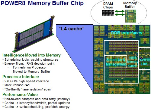
And here is how the memory subsystem using the Power8 dual-chip module (two six-core Power8sused in two-socket and four-socket machines) was assembled and the feeds and speeds thereof:

With 128 GB homegrown Centaur DIMMs (CDIMMs), IBM could support 1 TB of memory per socket.
With the jump from Power8 to Power9, IBM wanted to get hyperscalers and cloud builders on board, so it needed to move to more standard DDR4 memory, and with the Nimbus variant of the Power9, the company etched real and complete DDR4 controllers onto the chip and ditched the DMI SERDES circuits and the Centaur buffer chips. This had a couple of effects, the first of which being that IBM could only support 16 memory sticks per socket. The second effect is that the memory bandwidth has to go down.
With two bytes read and one byte written per channel per clock, the memory channels can sustain about 8 GB/sec of sustained memory bandwidth per channel between the processors and the Centaur buffer chip, which works out to an aggregate of 192 GB/sec of sustained memory bandwidth across the socket. The links between the L4 cache on the Centaur chip and the 32 total ports of DDR3 or DDR4 memory on the Power8 chip came in at a very high 410 GB/sec of bandwidth, helping to keep it all humming along.
With the Nimbus Power9 chips, the Centaur buffer is gone and sustained memory bandwidth drops to 150 GB/sec per socket, but with a 25 percent increase in the SERDES signaling in the DMI coming off the Cumulus Power9 chip, the buffered memory is now delivering sustained memory bandwidth of 230 GB/sec per socket.
Importantly, both are a lot better than what a “Skylake” Intel Xeon SP processor can do, whether IBM is using buffered or unbuffered memory. The 28-core Skylake Platinum chip does somewhere around 200 GB/sec to 230 GB/sec on a two-socket machine, depending on what part of the STREAM Triad curve you want to look at, call it 115 GB/sec per socket, on average, and IBM has a 70 percent advantage for unbuffered memory and a 100 percent advantage for buffered memory.
Now, here is where it gets interesting. Take a look at the Nimbus Power9 chip on the left and the Cumulus Power9 chip to the right:
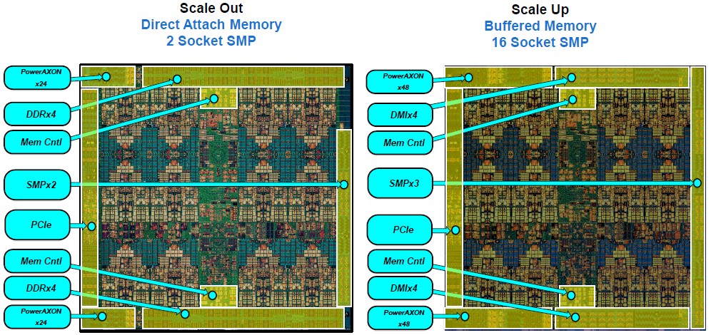
IBM is throwing a some new terms around here, and one of them is PowerAXON, and we hate that all caps a lot so we are never going to do it again. IBM used to call the 25 Gb/sec (25 GHz) signaling coming off the Power9 chip by the code-name “Bluelink,” just to keep it all straight. But AXON is an interesting name in that IBM uses the A Bus to designate NUMA links between server nodes in a big iron system and the X Bus to denote NUMA links coming off a processor within a single node. (IBM always says SMP when it means NUMA. This is not symmetric multiprocessing, but non-uniform memory access clustering.) The O is for OpenCAPI and the N is for NVLink. As that name suggests, IBM can tweak the speed and the protocol running atop the Bluelink SERDES to create memory links, NVLinks out to GPUs, OpenCAPI links out to other kinds of accelerators or storage class memory, X Buses for intranode hooks between processors, and A Buses for linking multiple nodes together. On the Cumulus chips, it looks like this:
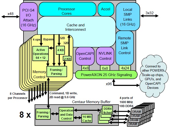
The PCI-Express 4.0 and X Bus for local NUMA links run at 16 GHz on the Power9 chip, saving a little heat, but the remote NUMA links as well as the NVLink and OpenCAPI links run at 25 GHz. The SERDES for the DMI memory interfaces on the Cumulus Power9 chip run at 9.6 GHz. Look at how small that DMI is on the Cumulus Power9 compared to the DDR4 controller on the Nimbus Power9. It opens up the chip to have a lot more I/O features while at the same time offering higher memory capacity and bandwidth per socket.
“There is a fundamental problem with DDR4 memory, and I am not sure how many people are aware of this, but the DDR technology with its single-ended, tri-state devices, are very hard to scale to large channels of memory or high frequencies,” Stuecheli explained in his presentation. “So we actually think that DDR memory is getting pretty close to end of life. So how do we get past that? We really want to attach our memory with a SERDES design, with differential signaling. If you look at the PHY area if a SERDES, it is much denser than DDR. So if we are going to attach a large amount of memory into our processor, we really need a SERDES solution. With buffered memory, you can do a SERDES to an intermediate chip and then let that buffer chip connect out to DDR devices. That is what we have done for quite some time.”
The architecture that IBM has set up with Power8 and Power9 chips confirms writes to DRAM – something that other architectures do not do, they just assume writes work – and that oddly enough means it is much easier to hook persistent memory into this more generic memory subsystem. The memory controller on the Power8 and Power9 chips is agnostic, and the Centaur buffer chip is created to talk either DDR3 or DDR4, and could also be tweaked to talk to future DDR5 or current GDDR5 frame buffer memory used in graphics cards, or any number of other persistent memories as they become available.
“This is a pretty dramatic difference,” Stuecheli continued in comparing the DDR4 controller in Nimbus to the DMI interface in Cumulus. If you look at the bit efficiency of DMI to DDR, per wire you are talking 10X the frequency, and it is differential so you have to divide it by two, but per pin, you have a 5X increase in bandwidth per chip floor area. So we really want to get to a SERDES solution to talk to the outside world.”
This all begs the question as to why all memory is not buffered as IBM and Intel have both done in their systems, and which would also possibly provide the physical mechanisms to disaggregate memory from compute and to make it all more composable.
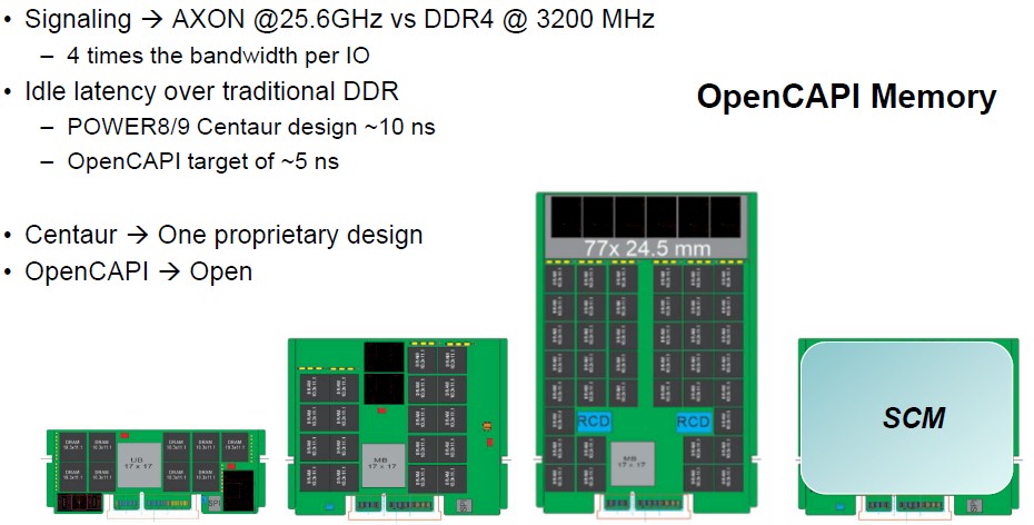
To that end, IBM is working with JEDEC, the DRAM memory standards body, to come up with a standard buffer that will adhere to its OpenCAPI protocol and that will eventually be put onto current DDR4 and future DDR5 memory. The Centaur memory adds about 10 nanoseconds of latency at idle compared to traditional DDR4 memory, which runs at around 100 nanoseconds when directly attached. This penalty is well worth it given the memory and bandwidth capacity increases that are possible with buffering. By eliminating the L4 cache on the Centaur, the buffer chip can be smaller and cheaper and IBM thinks it can get the latency overhead down to around 5 nanoseconds. That 10 nanosecond latency on the Centaur chip was one DMI port going to four DDR ports with a 16 MB cache lookup. The new design being done with JEDEC is for a single DMI port with a single DDR interface, so it is a much smaller chip without the L4 cache. “In our simulations with regard to loaded latency, it doesn’t take much load at all before this provides lower latency than direct attached memory,” said Steucheli.
IBM is impatient to test this idea out, and will be tweaking DDR4 memory and a Power9’ chip (that is a prime sign, instead of a plus) sometime in 2019 that will support this OpenCAPI memory approach. This is what was on that OpenPower roadmap from back in March, which was never fully explained, and here is it again:
“We are going to do another Power9 derivative chip with this new memory technology and there we are going to be able to deploy 350 GB/sec per socket of bandwidth,” said Steucheli. “And that is a more realistic system – we could actually do about twice that if we built more optimized memory buffers. If you an HPC vendor trying to speed up your simulations and you are disappointed by your bytes per flops ratio, that’s a pretty big improvement. We are taking what was in essence the Power10 memory subsystem and implementing it in Power9. With Power10, we will move up to DDR5 and that will push us up to about 435 GB/sec of bandwidth into our processor.”
[Note: The 210 GB/sec sustained bandwidth on the chart above for the Power9 Cumulus (SU) chip is wrong. It should be 230 GB/sec.]
If IBM could do twice the bandwidth again with more optimized buffers, then perhaps it should, because at that point it would be at the same bandwidth of the HBM2 memory used in GPU and vector accelerators and it would be linked to tens of terabytes of memory – three freaking orders of magnitude more than is available on those accelerators. (There is a very interesting CORAL-2 exascale possibility right there. . . .)
In any event, with Power10, IBM will jack up the signaling to 50 GHz for the Bluelink SERDES upon which this is all based, and PCI-Express 5.0 will also be on there, running at 32 GHz and twice as fast as the PCI-Express 4.0 used on the Power9. How many PowerAxon ports the Power10 chip has and how they are aggregated remains to be seen. That will depend on a lot of other factors.
This brings us to another point that illustrates the blurring between CPU and memory and accelerators, which Steucheli alluded to. If IBM wanted to – and we see no reason why it should not want to – it could create a killer four-socket Power9 machine not only with incredibly high memory bandwidth, but with a very large number of Bluelinks going out to accelerators or persistent memories. All of this would be founded on the Cumulus big iron NUMA server platform, which IBM announced earlier this month.
For review, here is the system topology of the big, bad 16-socket Power E980 system, showing the sockets and the buffered memory across four interconnected four-socket nodes:
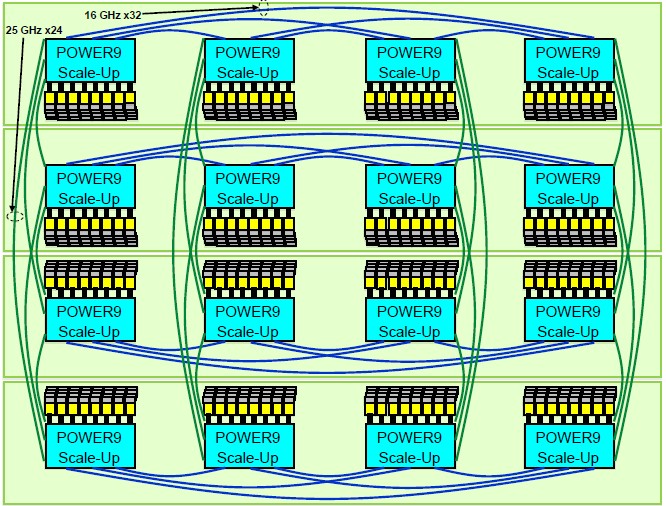
You can see the three X Bus links to hook the four sockets together, and each socket is only one hop away from any of the other sockets. The new X Bus links run twice as fast in the Power9 box as they did in the Power8 machines. There are four A Bus links coming off each processor, and these are used to cross couple as many as 16 sockets together such that any processor is no more than two hops away from any other processor in the complex; it is often only a single hop away. These A Bus links in the Power9 machines are four times faster than they were in the Power8 boxes. Add it up, this is a much tighter coupling of the processor complex, which should provide a big boost in performance above and beyond the architectural improvements in the Power9 cores and the increase in memory bandwidth from the new signaling.
Now, global replace all but the top four Power9 chips with Volta GPUs and convert the A Bus links to the NVLink protocol.
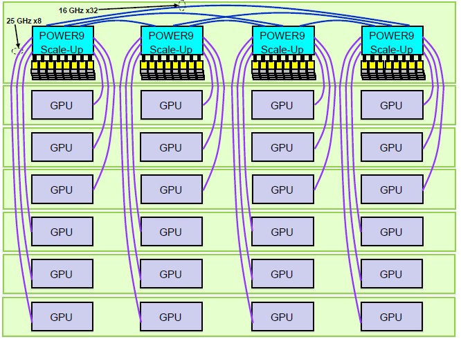
BAM! Just like that IBM could create its own DGX-2 in a heartbeat, with 24 GPUs in it, and have a hell of a lot more CPU memory bandwidth and also coherent memory across the CPUs and GPUs. The GPUs would be one or two hops away from any Power9 CPU. This would be a very interesting machine learning training machine, indeed. Why this machine does not already exist is a wonder. . . . Maybe it does, deep in the bowels of Google.
Or, you could take those Bluelink ports and burn the OpenCAPI protocol on them to directly attach NVM-Express flash, like this:
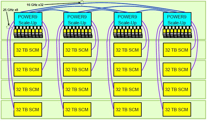
It is not clear why this theoretical system only has 16 flash drives instead of 24, but you get the idea. No matter what, this would be a very powerful and fast data analytics engine, we think. For all we know, this machine is also inside of Google, or something very much like it.

IO BW out of the CPU is key. IBM knows that and has lots of experience from Z business. POWER9 will rock!
Future of Power looks rather grim right now, especialy now that GF has confirmed it is basically stopping at 14nm and halted 7nm, IBM has to quickly find a new Foundry to continue.
GF has confirmed they’ll stop development of 7nm FF, they haven’t said anything about FDSOI, which is what IBM uses & has contracted GF for.
IBM itself confirmed to me that it was looking at foundries other than GF for Power10, and the only three options are Intel (well, its 10 nanometer) and we all had a laugh about that, or TSMC or Samsung. It will be Samsung. Power9 and Power9′ will be on 14 nanometer or 12 nanometer.
What about Global Foundries 12 nm FDSOI process? That would be a good fit for the 2019 refresh of POWER9.
PCIe gen 5 is 32Gb/s per lane (32MHz is a typo)
Interesting article at least in terms of discussing the Centaur Chip.
I admit that I have to read it again a few more times.
However, I believe the purpose of Centaur was to aid in IBM’s CUoD (Capacity Upgrade on Demand) implementation which allows ‘inactive’ or functionally useless memory capacity to be installed pending ‘activation’.
From an end-user point of view, the ability to have significantly discounted hardware installed pending either permanent or temporary activation was an innovative and bold step from IBM. They only charge you the difference if one decides to activate the physical resource.
But, back when IBM first started CUoD, the physical hardware FRUs and CCINs were distinct. These days they are co-mingled.
Consequently, and especially with the newer Industry Standard DIMMs, one can not determine if a specific DIMM Module is regular Plug and Play or has been firmware flashed as usable. This potentially impacts even CUoD unaware Systems.
Why is this a big deal?
Consider these current List Prices for the various P9 DIMMs (which are all the same per IBM)
——————————————————-
MT | FC | Description | List Price |
—–|——|—————————-|————|
9008 | EM65 | 128 GB DDR4 MEMORY | 5,599 |
9223 | EM6M | 128 GB DDR4 MEMORY | 5,599 |
8335 | EM65 | 128 GB DDR4 MEMORY | 5,599 |
9040 | EM6E | 128 GB DDR4 MEMORY (2666MH | 3,679 |
——————————————————-
Note the price diff for MT 9040. Per IBM, these are the same Industry Standard DIMMs as for all the other MTs. (same CCINs and FRUs)
Assume I have a 9223 and wish to populate all 32x DIMM Slots with 128GB. Why would I not find a friendly IBM BP and order the 9040 DIMMs, saving nearly $64K?
btw, it would not be difficult to do so.
Before anyone says ‘firmware’, assume we can already flash the DIMMs with 9223 compliant firmware. According to IBM, they already have that scenario covered.
So, assume we are 2 or 3 years ahead of 2019. 1 Year Maintenance has expired.
A user looking to recover asset investment trades out a used 9040 on the open market and the trader doing the ‘take-out’ legitimately advertises the FRUs and CCINs.
In every way, these DIMMs are identical to the Plug and Play DIMMs that a 9223 owner already sees as exiting on his/her own system.
But, per IBM, these are not enabled and only they know the difference.
So, the question is this.
What the hell are IBM thinking using the same FRUs and CCINs for both Plug and Play DIMMs and DIMMs that require Activation?
Certainly, we know that IBM wrongly perceive the secondary market as their competition. In doing so for the last 20 years, IBM’s Mid-Range market share has dropped from over 90% to less than 14%.
They have never once focused on their real competitors, who make Mid-Range Systems easier – not harder for end users.
In the scenario described above, IBM’s only answer is that it is their secret and the 9223 owner should be under IBM Maintenance, ordering the parts from IBM.
But, this is exactly the attitude which caused IBM to sign a consent decree back in the 1950’s, pledging to make FRUs and PNs available to end -users.
In the Mid 2000’s, IBM went back to Fed Court in New York and requested to be released from the consent decree, arguing that all PNs were now on-line and that they would continue to publish PNs and FRUs for the benefit of those end users who did not wish to be bound to IBM Maintenance.
With the previous P8 (and now P9) co-mingled CUoD memery chips (both IS and Custom DIMMs) it is my personal and professional opinion that IBM are looking to circumvent not only the intent of the original 1950’s consent decree, but they also materially mis-represented their intentions to the Federal District of New York when they petitioned to be released from the Consent Decree.
After all, if you have a bunch of different PNs that will only work based upon a secret code, it absolutely no different to the situation which the Court found so egregious back in the 1950s.
This may seem like a trivial concern for IBM bloggers who have little interaction at street level with real end users, but, I assure you it is a big deal for end-users when either Third Party Maintenance – or even recovery of asset investment (either for upgrades of resale) is dictated by a single monopolistic source.
Quite frankly, with IBM’s couldn’t care less attitude towards end-users, it is no wonder that they have lost money now for 26 straight quarters, nor that they needed nearly $2 Billion from Google to finish Power9.
And, while IBM’s vagueness regarding something as trivial as co-mingled P9 Plug and Play vs CUoD Memory modules may seem inconsequential, imho, it is absolutely symptomatic of the reason that so many have turned their backs on IBM as a viable Mid-Range solution.
Gary