Say what you will about the ruthless dominance of hyperscale companies, but they are managing to propel information technology at a rate, and in ways, that the enterprise and high performance computing markets can only dream of. Much of this is centered around demanding a lot more performance, a lot less cost, and higher energy efficiency from infrastructure componentry: processors, memory, local storage, and now networking.
Rajiv Khemani, co-founder and chief executive officer of Ethernet switch chip maker Innovium, has stated that the escalating rates of storage bandwidth and CPU performance in servers were some of the prime drivers at his company to build ASICs that would enable servers to share those resources much more efficiently across these large datacenter networks. Khemani reiterated those remarks at our recent Next I/O Platform event.
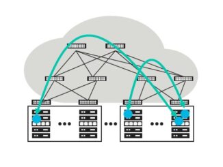
When we looked inside a server, he said, we saw that over the last decade and half, storage bandwidth had grown about 1,000X, thanks mainly to the transition from hard drives to flash. Over the same period Moore’s Law enabled CPU performance to multiply a couple of hundred times. At the same time, in most datacenters, connectivity had only progressed from 1 Gb/sec to 10 Gb/sec per second. “Network connectivity was the choke point,” explains Khemani.
According to him, one of the things holding back network performance was the fact the network chips sold into the datacenter were designed for legacy enterprise and telco environments. They decided they could do a lot better with a clean-sheet design that put an emphasis on modularity, programmability, and an efficient use of the transistor budget. As a result, they were able to make the data flow through the switch chip extremely compact and efficient, says Khemani.
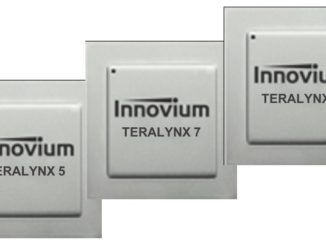
The first Teralynx switch ASIC was developed on 16 nanometer process technology, which kept costs down and reduced risk. Nonetheless, the hyperscale-targeted Teralynx 7 ASIC is able to deliver 12.8 Tb/sec of aggregate bandwidth and supports up 128 ports of running at 100 Gb/sec, 64 ports at 200 Gb/sec, or 32 ports at 400 Gb/sec. It is one of only a handful such chips in the switch market to reach those numbers, the others being Broadcom’s Tomahawk 3 and Trident 4 chips, Barefoot Networks’ Tofino 2 chip, and Marvell’s Prestera. The latter two rely on 7 nanometer technology to hit those speeds and port counts.
Innovium’s just-announced Teralynx 5 switch chip tops out at 6.4 Tb/sec and is aimed at top-of-rack switches and more modest-sized datacenters in enterprise, edge, and 5G environments. It supports the same range of port speeds as the Teralynx 7 (as well as 10 Gb/sec, 25 Gb/sec, and 50 Gb/sec ports, but at half the number of ports as the Teralynx 7.
In future products, Khemani said they think they will be able deliver the same feature set of the original products, but at speeds of up to 51.2 Tb/sec “without having to do crazy changes to the architecture or significant risk in terms of the design.”
According to Khemani, they will use a few different technology vectors to hit that level of performance. One of those vectors is Moore’s Law and its magical shrinking transistors. At 5 nanometer and 3 nanometer transistor geometries, he believes they will be able to attain 1.6 Tb/sec port speeds (assuming there’s an Ethernet standard in place when that happens). Beyond that, he said they are working with Molex on a system design that will enable better SerDes performance. Khemani also thinks 800 Gb/sec pluggable modules are “just around the corner” and believes initial samples will show up sometime next year. Further down the line, he expects to see photonic switching, a technology that many believe will enable disaggregation of server processors, memory, and storage.
“The next few years are going to be really exciting in that we will be able to solve all of these challenges,” said Khemani. “The network will be able to free up innovation inside the server node.”


Be the first to comment