Cash used to be king, and now market capitalization is. That’s one of the reasons that the biggest players in the semiconductor arena are snapping up competitors, startups, and suppliers in adjacent chip markets at an increasing pace and with very large bags of “money.” Stock isn’t quite bitcoin, which doesn’t have an initial cap like dollar, euro, renminbi, or yen, but it rises and falls like bitcoin, is not a real currency either, and it can be almost as ephemeral. You might as well spend it while you got it, and companies that are being acquired might as well take it as it is being offered.
And that is one of the reasons why chip maker Marvell has just acquired Innovium, one of the up and coming suppliers of high-end Ethernet switch ASICs, one that has focused almost exclusively on hyperscale and cloud builder datacenters and has expanded recently into edge use cases.
Innovium was founded in 2015 and dropped out of stealth in March 2017, when we did our initial profile of the company. The company was co-founded by three people with deep expertise in datacenter networking. Puneet Agarwal, who is chief technology officer, and Mohammad Issa, who is vice president of engineering, started Innovium to minimalize the protocol stack on switch ASICs and to really push Ethernet to higher bandwidths. It is significant that Agarwal was CTO for switching at Broadcom, the merchant switch silicon leader for datacenter switching, for more than a decade and that Issa was vice president of engineering there as well; they drove Broadcom’s “Trident” and “Tomahawk” switch ASICs, which are the foundation of hyperscale and cloud builder networks to this day, despite very intense competition from a slew of upstarts. Rajiv Khemani, Innovium’s chief executive officer and the third co-founder, ran Intel’s network processing business for a bunch of years and then was chief operating officer at Cavium.
That, in hindsight, is probably also a significant fact. Marvell acquired Cavium in November 2017, which not only gave Marvell the ThunderX Arm server CPUs but also the XPliant programmable switch ASICs that were groundbreaking in their approach to programmability. XPliant was founded in 2011, two years before Barefoot Networks (now the foundation of the Intel datacenter Ethernet switching business), and dropped out of stealth mode with its first switches in 2014. At the time, Marvell had its own Prestera line of Ethernet switch ASICs, and after the Cavium acquisition closed, created a $3.4 billion company chasing a $16 billion total addressable market for semiconductors across the datacenter, edge, and embedded markets (and only about 10 percent of that revenue was hitting that TAM, so there was a lot of room for growth), the XPliant switches took a backseat and the Prestera line, which was really focused on carrier and campus networks and has been expanded out to the edge as that has become fashionable and over into the large enterprise.
In the intervening years, the ThunderX chips are no longer commercially available – but can be customized if someone wants them and are part of the mass customization chip business that Marvell is trying to architect as it takes on Intel, Broadcom, AMD, and others for its slice of the semiconductor pie. And maybe the acquisition of Cavium had more to do with Ethernet adapters and CPUs and storage adapters and less about datacenter switching.
In a sense, Marvell has decided that it needs something to fill in the hole that it thought it had plugged so many years ago with the XPliant ASICs and that it has stretched the Prestera line in recent years to try to cover. While the Prestera line accounts for tens of millions of ports sold across more than a hundred customers, it is not the right ASIC for hyperscalers and cloud builders who need more bandwidth and lower latency – and at what we presume is a lower cost per bit moved, too.
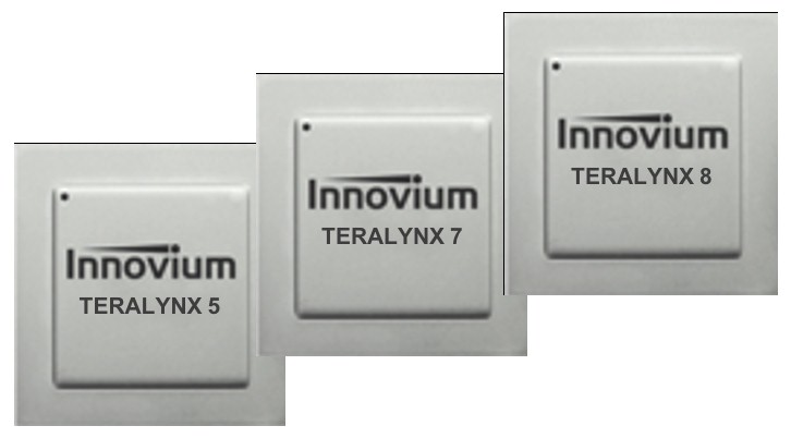
Innovium unveiled its Teralynx 7 ASIC at launch in 2017 and started shipping the chip at the end of 2019. The Teralynx 7 chip came in 3.2 Tb/sec, 6.4 Tb/sec, and 12.8 Tb/sec aggregate bandwidths aimed at top of rack, leaf, and spine switches. That top end Teralynx 7 chip was able to drive 128 ports running at 100 Gb/sec, 64 ports running at 200 Gb/sec, or 32 ports running at 400 Gb/sec, and it had an embedded Arm core for running network telemetry and analytics processing engines to monitor and shape network traffic. The architecture also had a programmable forwarding plane without having to go all the way to full programmability in the P4 language as Barefoot Networks has done with its “Tofino” line of Ethernet switch ASICs. The important thing was that Innovium was delivering 200 Gb/sec and 400 Gb/sec ports when other vendors were pushing 100 Gb/sec ports and only talking about 200 Gb/sec ports.
In September 2019, at our Next I/O Platform event in San Jose – remember when we went to live events? – Innovium launched its Teralynx 5 switch ASIC, sporting a new Teralynx architecture that allowed Innovium to scale a chip down as low as 1.2 Tb/sec and as high as 51.2 Tb/sec of aggregate bandwidth. The Teralynx 5 chip had 128 SerDes compared to the 256 SerDes in the Teralynx 7, and therefore had a lower 6.4 Tb/sec peak aggregate bandwidth in the family. But each SerDes in the Teralynx v2 architecture was half as big, which means twice as many could be crammed into a given chip area. Both chips were implemented in the mature 16 nanometer processes from Taiwan Semiconductor Manufacturing Corp, and this is important because Innovium could save a jump to 7 nanometer processes to further increase SerDes density and therefore aggregate bandwidth per ASIC.
In May 2020, Innovium expanded up the Teralynx architecture and created the Teralynx 8 chip, which had 25.6 Tb/sec of aggregate bandwidth and could drive 256 ports at 100 Gb/sec, 128 ports at 200 Gb/sec, 64 ports at 400 Gb/sec, and 32 ports at 800 Gb/sec. This chip marries TSMC’s 7 nanometer processes with the Teralynx v2 architecture that debuted in the Teralynx 5 chip, and that’s how it can drive so many ports at such high speeds. As with other network chip makers, the increasing bandwidth of the devices allows for an increasing radix – port count at a set bandwidth – and at 100 Gb/sec speeds, which is good enough for a lot of workloads in the datacenter, it takes one-sixth the number of Teralynx 8 devices to drive 256 ports instead of six interlinked Teralynx 7 ASICs. The Teralynx 8 no doubt costs a lot more per chip, but the cot per bit can come down at something closely approximating Moore’s Law. And the aggregate wattage goes way down, too, as you reduce the number of chips. Innovium no doubt has a Teralynx v3 architecture in the works and a process shrink to 5 nanometers to push the bandwidth and radix envelopes even further.
This time last year, when Innovium raised $170 million in Series F financing – it is rare to see so many rounds before a company is either bought or goes public – it had raised a total of $350 million in its six rounds of funding. That gave Innovium unicorn status, with a valuation of $1.2 billion this time last year. The actual valuation – which we put more stock into (pun intended) – came pretty close to the theoretical one. But none of it is cash.
In a statement announcing the deal, Marvell said that Innovium still had $145 million of that cash on hand, and that the $1.1 billion all-stock acquisition will really only be a net cost of $955 million. The way we look at it, Marvell had a market capitalization of $49.6 billion when the deal was announced, told Wall Street it was going to dilute its shares by 19.05 newly issued shares, and the market capitalization went up since then by $1.97 billion. Marvell gets to keep the $145 million in cash, and the news of the acquisition drove another $870 million in market capitalization.
What an amazing world we live in.
Agarwal will be joining Marvell as part of the deal, which is expected to close by the end of the year, and so will the rest of the Innovium team. Khemani will serve as an advisor to Marvell after the deal is done, but will not be a manager or any other kind of employee of Marvell.
Marvell said that the market for Ethernet switch ASICs in the datacenter is expanding at a compound annual growth rate of 15 percent and is expected to reach $2 billion by 2026. Marvell added that one of the big clouds (a Tier 1, as they sometimes say) had selected Innovium to be “a significant supplier” and that other clouds (which we presume also includes hyperscalers that don’t have clouds) are engaged with the company for its Teralynx chips. The way we see it, being part of Marvell makes Innovium a safer bet, just like Cray being part of Hewlett Packard Enterprise did. After HPE bought Cray, the venerable supercomputer maker was able to close a slew of pre-exascale and exascale supercomputer deals that, we think, it would never have been able to do without HPE’s relatively deep pockets and strong relationships in the semiconductor supply chain. We suspect that those spending big bucks knew such a deal was happening, in fact, and this may also have been the case with Marvell and Innovium and that Tier 1 that remains unnamed. (We suspect it is Amazon Web Services.)
The Innovium Teralynx line will be rebranded the Prestera 9X, and is expected to drive around $150 million in sales in 2022 and will sit beside the existing Prestera 2K through 8K lines. Marvell now has a better way to take on Broadcom’s Trident and Tomahawk, Intel’s Tofino, Cisco Systems SiliconOne, and Nvidia Spectrum ASICs to get a piece of that $2 billion action.


Great coverage. Beyond even what the article covers, I believe the longer play is that this acquisition along with Inphi. The combination of these two acquisitions sets up Marvell to incorporate on board optical processing with their switch silicon to compete at the high end of the multi-terabit switch market, similar to Broadcom is doing with their silicon, and what Cisco is contemplating with their nextgen SiliconOne processor combined with Acacia optics. This is the beginning of full integration between optics and silicon in the multi-terabit switching space.