
Bringing a new switch ASIC to market is no easy task, and it isn’t cheap, either. It is even harder to do without riding on the Moore’s Law curve down the process shrinks, but this is what upstart chip maker Innovium has just done.
The founding premise of Innovium, one of the upstart switch chip makers that jumped straight to 200 Gb/sec and 400 Gb/sec switching with its initial Teralynx 7 chip that was announced two and a half years ago, was to do it lean, and mean, and fast, beating upstart rivals Barefoot Networks (now part of Intel) and the XPliant division of Cavium (now part of Marvell) in the race for 12.8 Tb/sec devices and to also stand toe-to-toe with Broadcom, the former employer of the key chip designers working at Innovium.
The Teralynx 7 chip will be in volume deployments at a number of hyperscalers and cloud builders by the end of this year. Significantly, Cisco Systems has ported its NX-OS network operating system to the Teralynx 7 chip, and is using this ASIC in its Nexus 3408 and Nexus 3432 switches. Microsoft’s SONiC network operating system and abstraction layer has also been ported to the Teralynx 7. This is about as close to hitting a home run as anyone can do against the likes of Broadcom, which basically owns the merchant switch ASIC business for datacenter networking.
Not content to rest on its laurels and savvy enough to know that Broadcom will respond and so will Intel and Marvell, the chip designers at Innovium are going both broad and deep with a crank on the Teralynx architecture, setting themselves up to compete at the 25.6 Tb/sec and 51.2 Tb/sec bandwidth stops on the datacenter switching roadmap. Broadcom is figuring to hit 25.6 Tb/sec with its “Tomahawk-4” chip, which we hear is taping out now and will probably revealed in early 2020, delivering 128 ports running at 200 Gb/sec. This will presumably be followed up by the “Tomahawk-5” two years later, delivering 128 ports running at 400 Gb/sec thanks to that 51.2 Tb/sec of aggregate bandwidth.
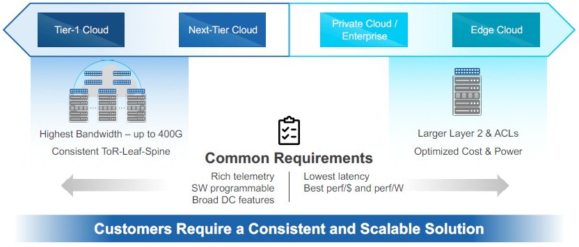
These and other chips, such as the “Trident” enterprise and “Jericho” deep buffer switch ASICs from Broadcom, are what Innovium is targeting with its Teralynx v2 architecture, with the first instantiation of that architecture being the Teralynx 5, aimed more at the Trident family as well as extending down into edge use cases. Switch chip makers are notorious for not being specific about their architectures (in stark contrast to CPU, GPU, and FPGA makers), but Rajiv Khemani, co-founder and chief executive officer at Innovium, tells The Next Platform that the new Teralynx v2 architecture has more than 40 patents added to its existing portfolio of 30 patents that were related to the Teralynx v1 architecture embodied in the Teralynx 7 chip.
The new patents relate to architecture, data structures, algorithms, and in-line telemetry. One of the key things Innovium’s engineers focused on was tweaking the design so it could jack up the performance by 2X within the same area, and that has allowed for Innovium to hang back on the 16 nanometer process node at Taiwan Semiconductor Manufacturing Corp while other switch ASIC makers are pushing into the more advanced (and more expensive and more risky) 7 nanometer process. Moreover, the Teralynx v2 architecture and the Teralynx 5 ASICs that employ it can be etched on a monolithic die and Innovium does not have to resort to using chiplets for switch cores.
In other words, Innovium can save that chiplet trick for a future day, perhaps with its Teralynx v3 architecture when the 7 nanometer processes are more mature and less expensive than they will be this year and next.
The biggest change, perhaps, with the Teralynx v2 architecture is that it is modular, and is explicitly meant to scale from devices that need as little as 1.2 Tb/sec of aggregate switching bandwidth to as much as 51.2 Tb/sec with a future behemoth, presumably to be called the Teralynx 7+ or Teralynx 7S at some point down the road. We figure that the Teralynx v2 architecture can be used to double up the top end chips aimed at hyperscalers to 25.6 Tb/sec using 7 nanometer TSMC processes (call that the Teralynx 7+ line), and then double it again to 51.2 Tb/sec by shrinking chip processes further at some future date (call that the Teralynx 7S). The point is to think of chip families, Teralynx 5 and Teralynx 7, aimed at different parts of the market and all based on a single, modular architecture that gets enhanced over time. This is different from the way Broadcom is making its Trident, Tomahawk, and Jericho ASICs, which address different parts of the datacenter switching market with different ASICs with some commonality. In fact, Innovium is trying to do with two families with one architecture what Broadcom does in three architectures. We shall see which strategy will win out.
“Using the data galaxy analogy that The Next Platform talks about, there will be big datacenters in the heart of the galaxy and smaller ones out in the arms and spreading out between them, too,” says Khemani. “And to address these diverse needs, the design needs to be very modular. If you have to have a brand new architecture for each place in the data galaxy, it’s just not feasible. But with the new Teralynx v2 architecture, we can scale down as low as 1.2 Tb/sec and up to 51.2 Tb/sec and beyond. That is a tremendous accomplishment and we think a multi-generational advantage for us as we execute on multiple products in the coming years.”
The Teralynx 5 has flexible SerDes circuits, just like the Teralynx 7 did, which means it can support 10 Gb/sec or 25 Gb/sec lanes using NRZ encoding or an effective 50 Gb/sec per lane using PAM-4 encoding, which allows two bits to be transmitted per signal. The Teralynx 7 had 256 SerDes, and the Teralynx 5 has 128 SerDes, which explains the difference in the aggregate bandwidth of 12.8 Tb/sec and 6.4 Tb/sec for each family. (The difference is that it takes half the area for each SerDes in the Teralynx 5 as it did in the Teralynx 7, which means the architecture can scale up to twice the performance in the same area as the Teralynx 7, which puts it at 25.6 Tb/sec of aggregate bandwidth in that future Teralynx 7+ chip as we are speculating about above.
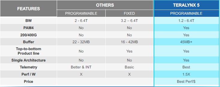
The Teralynx 5 chips are fully software compatible with the Teralynx 7 chips, which means all of the network operating systems that have been ported to the latter will work on the former without having to tweak the code. The Teralynx 5 is interesting in that it will have a buffer weighing in at more than 45 MB – Innovium won’t say how big it is – compared to the 70 MB buffer on the Teralynx 7. The updated architecture has ingress access control lists that are 4X bigger than at the same aggregate bandwidth with the prior architecture, and the MAC table sizes are 2X bigger. That’s pretty impressive without a process shrink from TSMC.
It looks like Innovium was saving some area tricks for later when it did the Teralynx v1 architecture.
Here is how Innovium is stacking itself up against the competition, vaguely and without naming names:
Support for the RoCE v2 implementation of RDMA for Ethernet is not mentioned in this table, but the Teralynx switch ASICs support this protocol for reducing latency, and this is one of the reasons why the Teralynx chips can get down to 400 nanoseconds on a port-to-port hop.
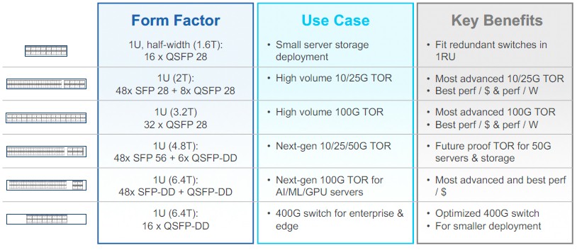
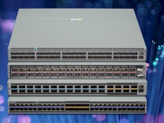
Innovium expects for the Teralynx 5 to be deployed in a number of different form factors and in a number of different scenarios in the datacenter. Here are the expected popular form factors:
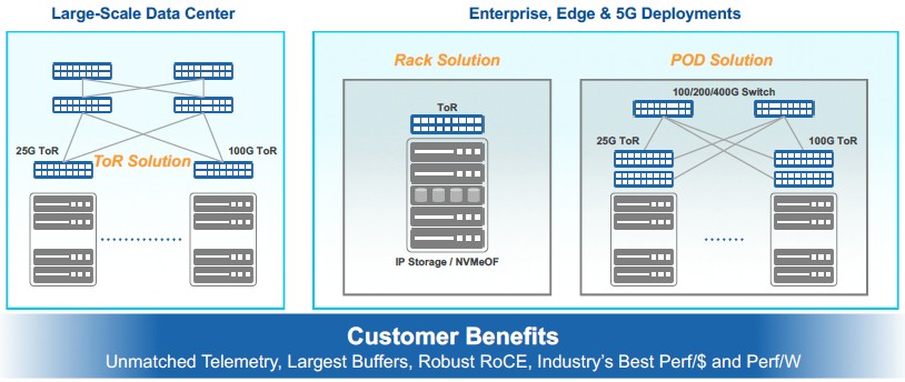
And here are the expected popular scenarios:
The Teralynx 7 came in three varieties – with 3.2 Tb/sec, 6.4 Tb/sec, and 12.8 Tb/sec aggregate bandwidth. The Teralynx 5 basically replaces the bottom two chips, and then extends it down with a new lower end chip that runs at 1.2 Tb/sec. Switch makers can dice and slice that bandwidth into ports that run at 10 Gb/sec, 25 Gb/sec, 50 Gb/sec, 100 Gb/sec, 200 Gb/sec, or 400 Gb/sec as they see fit in various products they want to bring to market, and this time around, the Teralynx 5 will be half the cost per bit transferred compared to alternatives in the market. That sounds like a pretty good deal, and it is exactly what the hyperscalers and cloud builders expect for their leaf or top of rack switches. That this was done without a process shrink is remarkable, truly.
The Teralynx 7 will be relegated to the role of a spine or core switch ASIC, which is fine. It will be upgraded at some point, too. All of the four different Teralynx 5 chips are pin compatible with each other, but they are not pin compatible with the Teralynx 7 as far as we know.
The Teralynx 5 chip will start sampling in the fourth quarter, which just started, and Innovium is taking orders for evaluation chips now. The chip is expected to start appearing in evaluation systems in the first quarter, and will make their way into commercial products throughout 2020 if all goes well.




Be the first to comment