
Nvidia launched its second-generation DGX system in March. In order to build the 2 petaflops half-precision DGX-2, Nvidia had to first design and build a new NVLink 2.0 switch chip, named NVSwitch. While Nvidia is only shipping NVSwitch as an integral component of its DGX-2 systems today, Nvidia has not precluded selling NVSwitch chips to data center equipment manufacturers.
This article will answer many of the questions we asked in our first look at the NVSwitch chip, using DGX-2 as an example architecture.
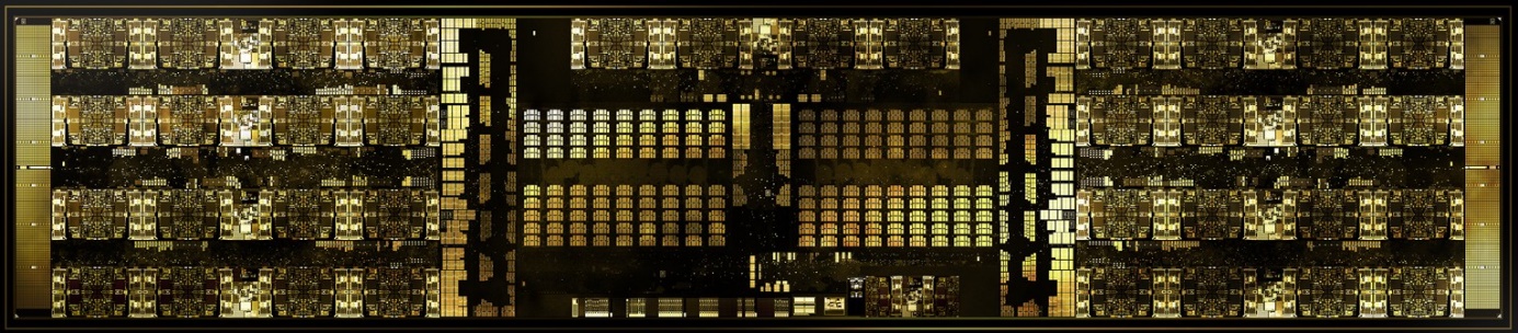
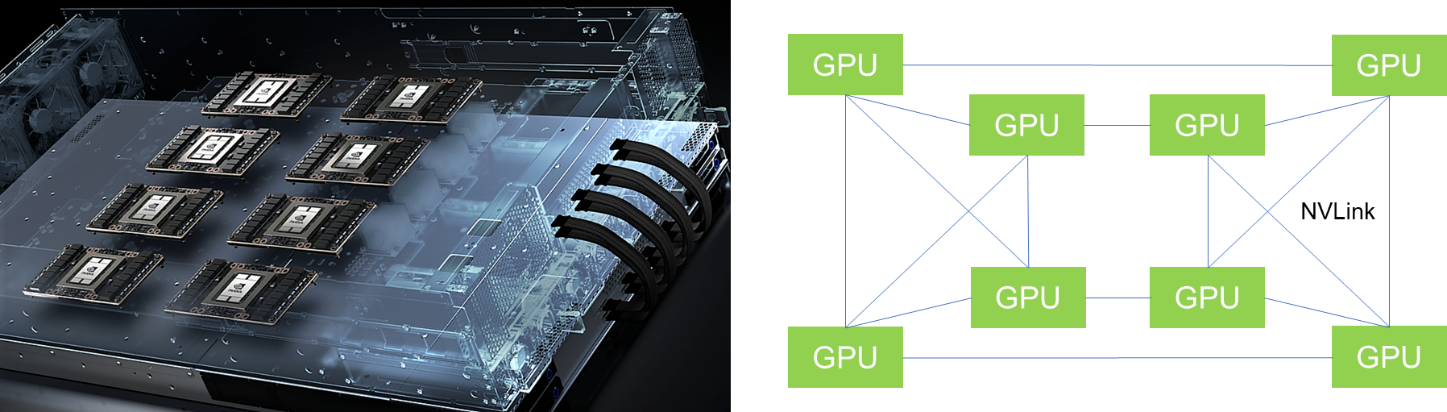
Nvidia’s NVSwitch is a two-billion transistor non-blocking switch design incorporating 18 complete NVLink 2.0 ports operating at a full 25 GB/sec bi-directional throughput per port (for a total of 50 GB/sec per port). Its 4 centimeter square ball-grid array (BGA) package has about 1,940 pins. About 30 percent of these are NVLink lanes (576), the rest are for power delivery, health monitoring, and the like.
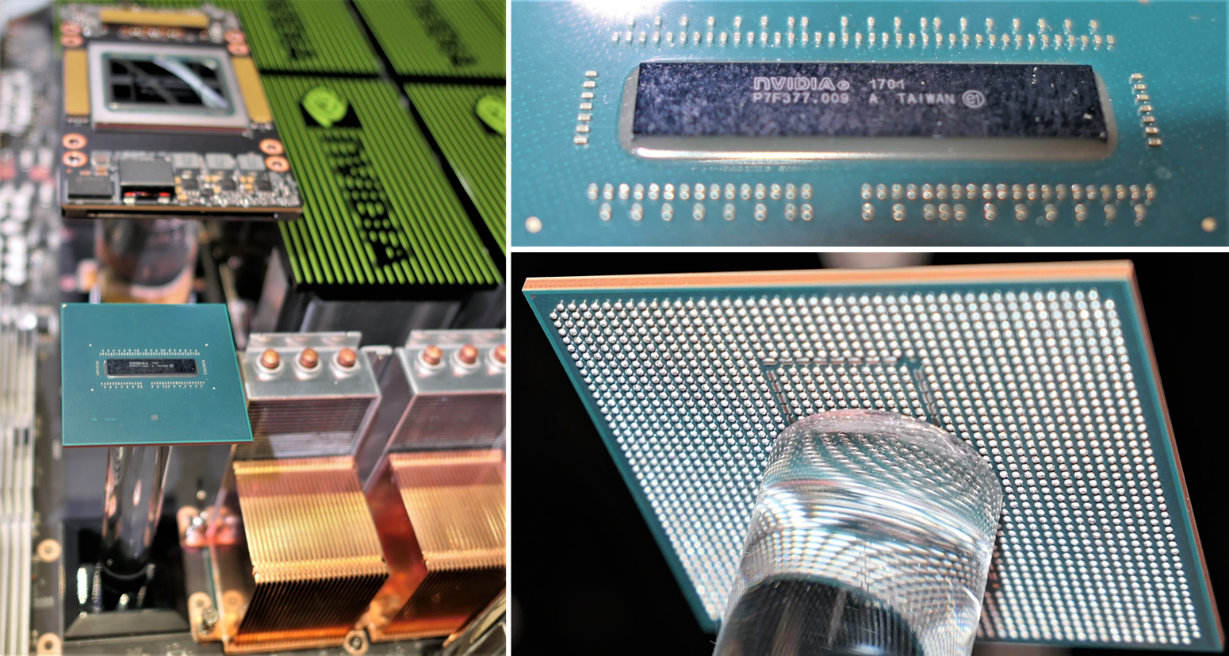
NVSwitch consumes less than 100 watts per chip. Its power consumption is mostly dependent on powering the external interfaces, so the more NVLink ports are connected, the more power it consumes. The power budget works out to perhaps 5.5 watts per full bi-directional NVLink port.
NVSwitch can therefore handle 450 GB/s of bi-directional traffic (900 GB/sec adding up both directions). The chip is laid out so that there are 8 ports on each end of the chip, with 2 ports in the middle (above center in the die photo).
DGX-2 System Design
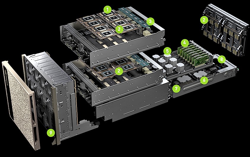
Nvidia’s DGX-2 design is massive and complex. At GTC, Nvidia showed a physical version of its website’s exploded diagram.
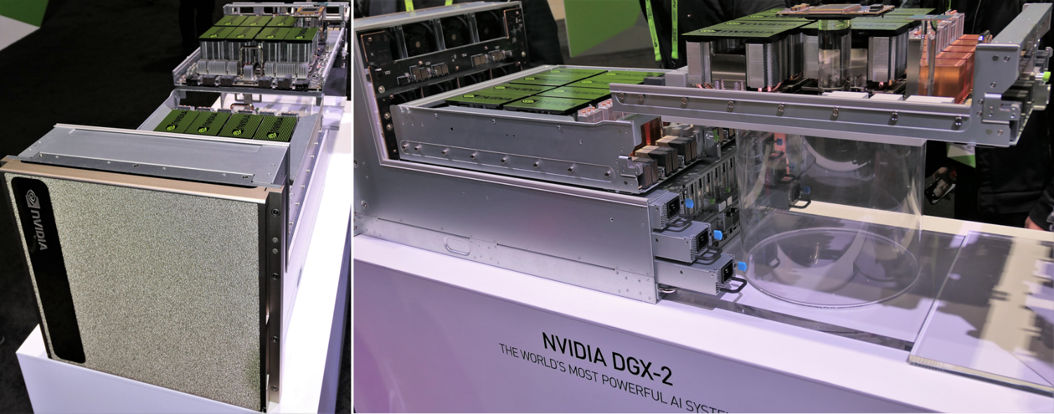
At 10U tall, the system cross-section is almost square (18-inches tall by 19-inches wide). There are four sub-chassis with motherboards:
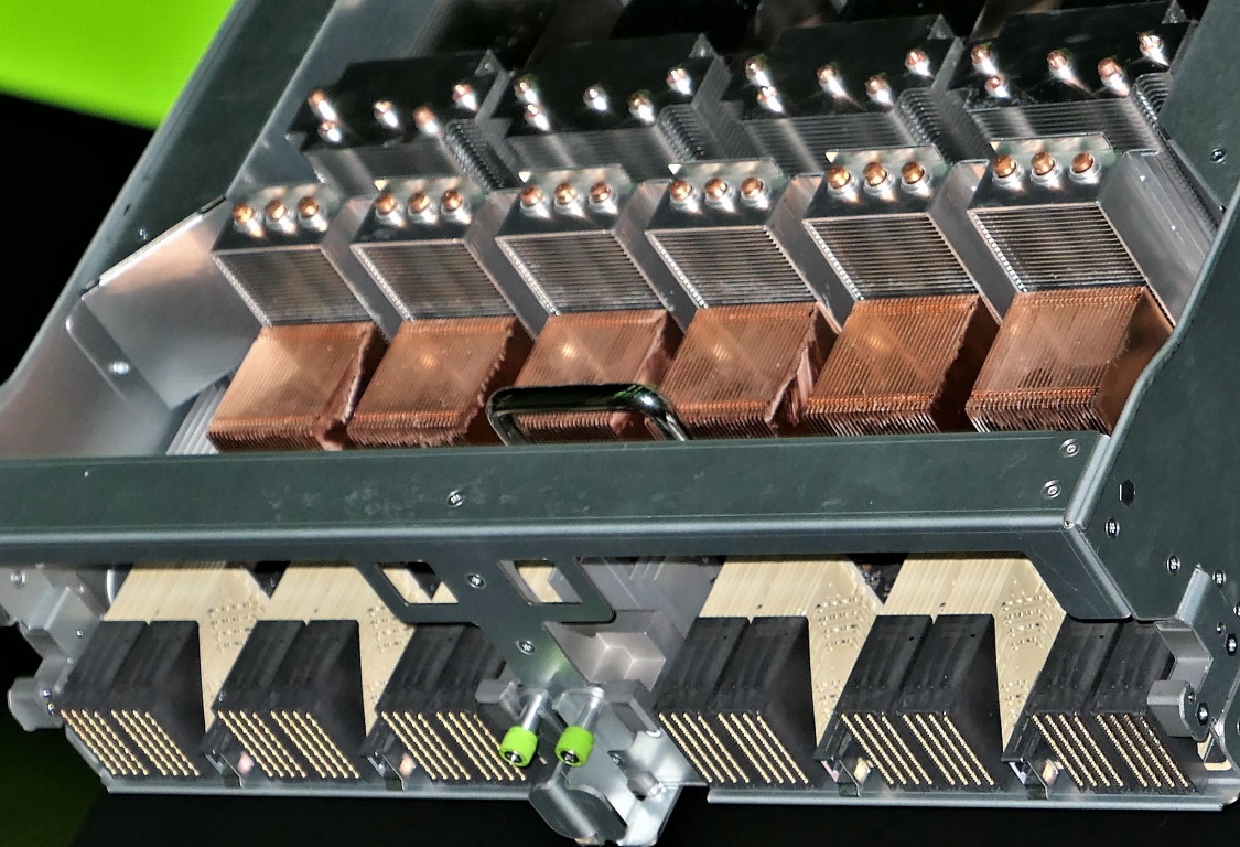
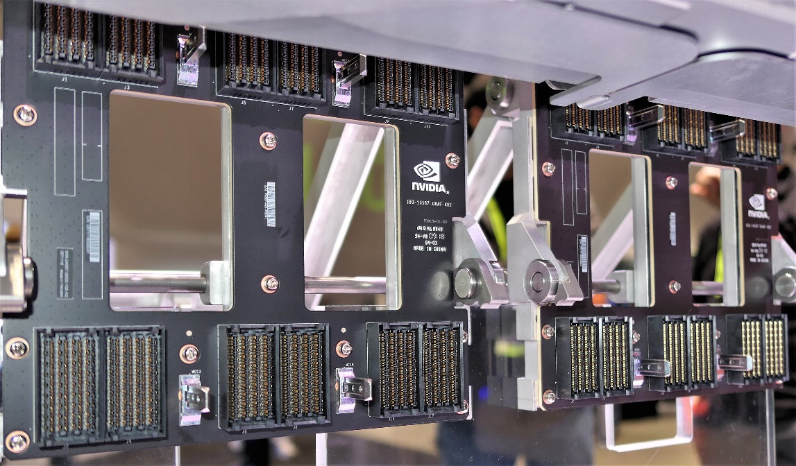
- Two identical 3U GPU sleds, each housing eight Tesla V100 32 GB SXM3 GPU modules (the new ones) and six NVSwitches
- A 2U server sled with two Intel Xeon Platinum processors, 1.5 TB system memory, and dual 10/25 Gb/sec Ethernet NICs
- A 2U interface sled separating the server sled from the GPU sleds, containing 12 PCI-Express 3.0 x16 switches and slots for eight PCI-Express 100 Gb/sec network interface cards (NICs)
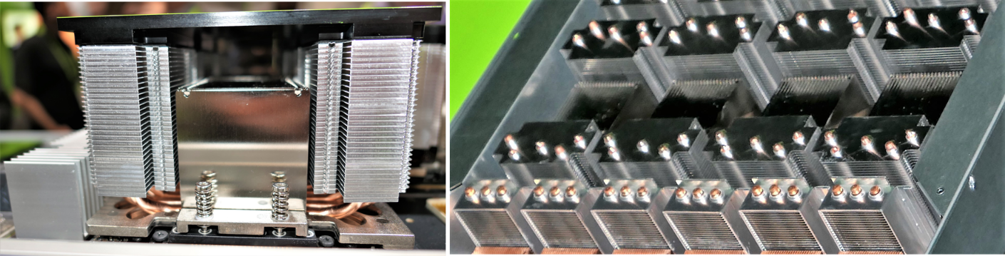
The Tesla V100 32 GB SXM3 GPU modules still use NVLink 2.0, but are rated for higher power consumption and sport a new air-cooled heat sink (more on that below). The combined memory space of the GPU’s on-board high bandwidth memory (HBM) is half a terabyte.
The chassis front panel houses 30 TB of NVMe SSD capacity across eight drives, which can be doubled up using fatter SSDs to 60 TB. DGX-2 is configured with eight 3.84 TB NVM-Express SSDs populated, out of sixteen available SSD bays.
DGX-1 Interconnect Topology Refresh
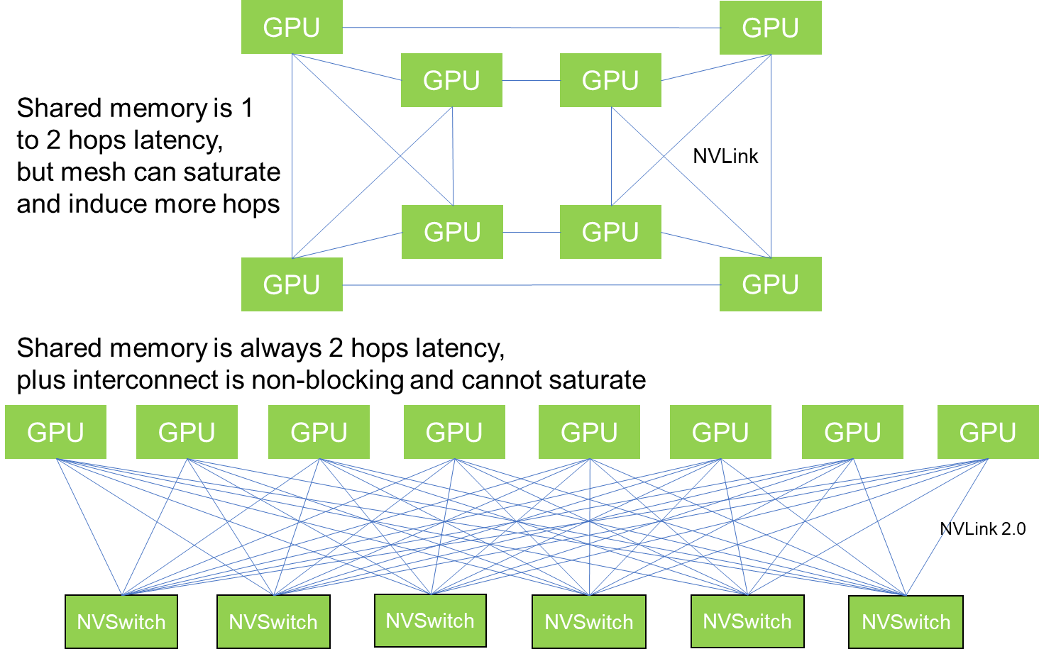
Nvidia’s original DGX-1 system connected eight Tesla P100 SXM2 GPU modules in a partially connected cube. It is a partially connected cube because each P100 SXM2 module has four NVLink ports – a fully-connected cube could be constructed if each GPU module had eight NVLink ports, but that would make the SXM2 module prohibitively expensive for more common configurations of two to four GPU modules per system.
The DGX-1 connects its dual-processor server with the GPU complex via PCI-Express switches in what is essentially an overlay network. Each SXM2 module integrates a single-host PCI-Express 3.0 x16 connection (fewer lanes can be used, but only one link is possible). Nvidia connected two GPUs to each PCI-Express switch in the following configuration:
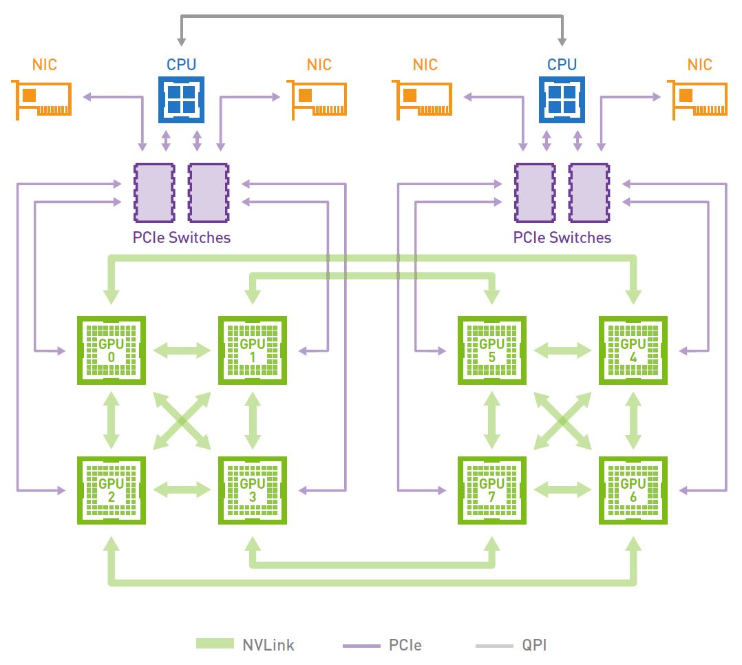
GPU to GPU memory transfers via NVLink are at most two hops away – a memory request may have to be routed through the NVLink controllers on two GPUs. In the above diagram, GPU 0 may need data in GPU 5’s memory. The non-NVLink connected GPUs communicate via PCIe access, which is much lower bandwidth and longer latency. Each NVLink controller has a memory access latency, so latency multiplies via the number of hops. Memory transfers between server system memory and GPU module memory take place over the switched PCI-Express interconnect, which is slower than NVLink.
Nvidia’s DGX-2 system design uses twelve NVSwitch chips and sixteen of each NVSwitch chip’s ports. The result is a high-speed switched interconnect fabric with 2.4 TB/sec bisectional bandwidth. But what does that mean, practically speaking?
NVSwitch routing latency is the same as a GPU’s SXM2 or SXM3 NVLink 2.0 controller’s routing latency. The physical layer latencies between NVLink 2.0 devices are the same as well.
Each GPU board hosts eight GPU modules and six NVSwitch chips. Nvidia upped the NVLink port count on its Tesla V100 SXM3 GPU module to six ports (there is still only one PCI-Express 3.0 x16 host interface). Each GPU connects directly to all the NVSwitch chips on the board, using one NVLink port to connect with each NVSwitch chip. Each NVSwitch therefore uses eight NVLink ports to connect to the GPUs on the same board.
This topology fully-connects all eight GPUs on a single board with a consistent two hops for each remote memory transfer. The first hop is from a GPU to an NVSwitch, the second hop is from the NVSwitch to the target GPU.
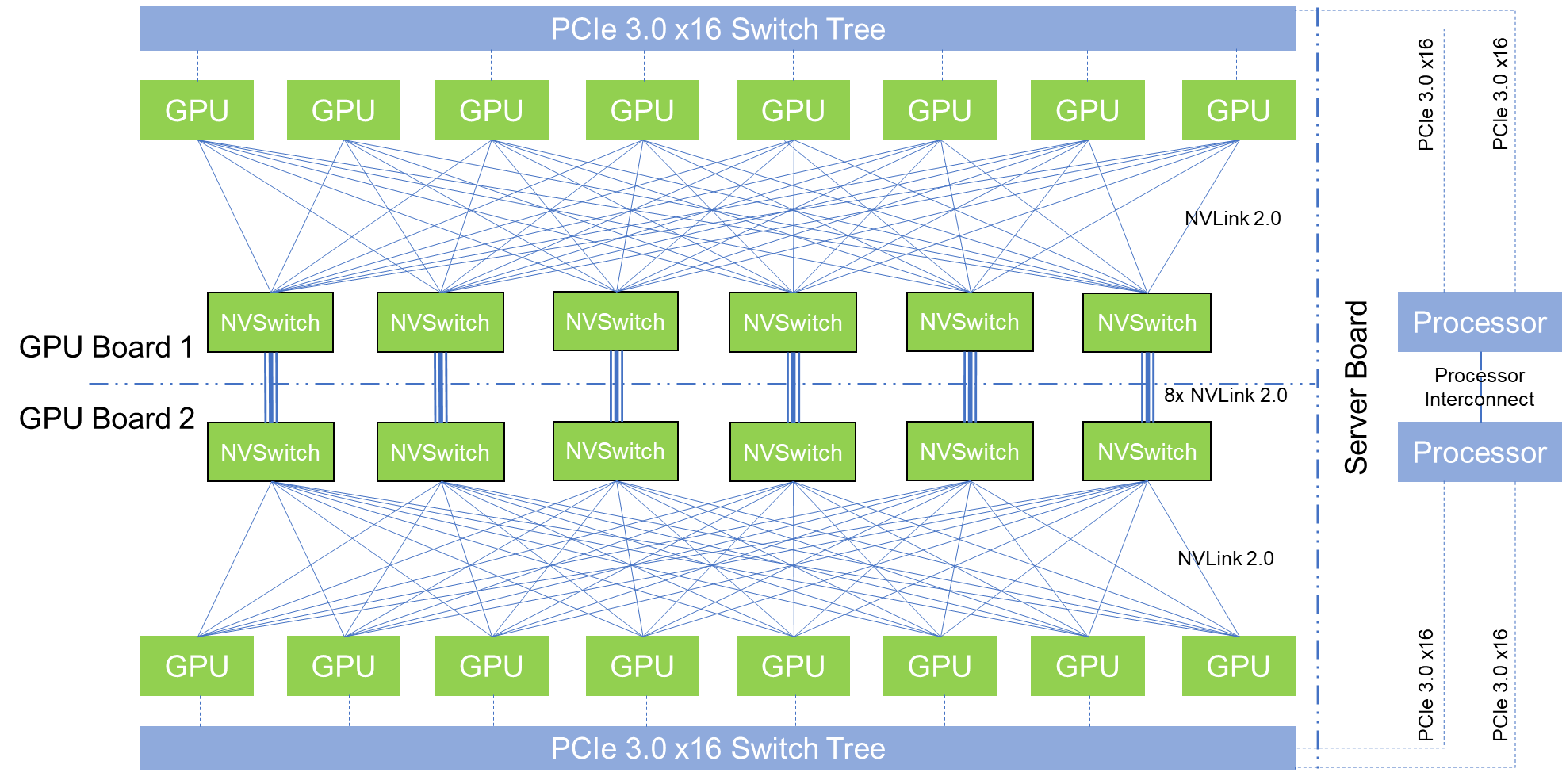
The two GPU boards are connected via the NVSwitches. Each NVSwitch is connected directly to its counterpart NVSwitch on the other board. These connections are eight NVLink ports wide, which brings the total NVLink ports used to sixteen per NVSwitch.
A GPU on one board will see a maximum of three hops to access memory of any GPU on the other board. There is no difference in latency to bridge between NVSwitch chips (and therefore between boards), so there is about a 50 percent latency penalty for the extra hop.
The DGX-2 NVSwitch topology is non-blocking. Each NVSwitch has the bandwidth to directly pass through all its traffic to target destinations without needing to implement flow control. The only part of this topology that can saturate is a GPU module: if six or more GPUs simultaneously request large chunks of data from a single other GPU’s memory, it could saturate the six NVLink connections for that single other GPU.
The result is not just a unified memory space among GPU modules, but a lower average hop count and more consistent remote memory access latency model than other topologies would enable. It also uses the fewest NVSwitch chips possible to achieve this efficiency.
In the above diagram, we made one concession for readability – the PCI-Express 3.0 x16 switch trees are on a fourth board. While Nvidia has made only a partial rendering available for that board, we speculate that there are twelve PCI-Express 3.0 x16 switches on that board:
- Eight PCI-Express switches connecting the processor board to the two GPU boards holding 16 GPUs, keeping the 2:1 ratio from the DGX-1
- Four PCI-Express switches connecting to two NICs each, which supports full 100 Gb/sec bi-directional network connectivity through the PCI-Express switch complex to the processor board (EDR InfiniBand has the same bandwidth as 100 Gb/sec Ethernet)
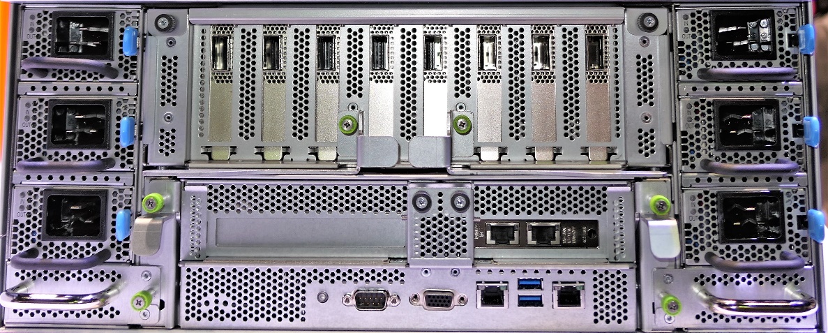
A Brawny Chassis
Every single electrical connection has a mechanical insertion and removal force, no matter how small or seemingly inconsequential. In a server, connectors are clustered for electrical layout convenience, to control cable connector costs, and to reduce assembly complexity. Connector size is limited to ensure that cables can be:
- Easily inserted into their connectors by people and/or cost-effective robots during the assembly process and
- Removed and reinserted by people in the field (a data center) if repair is needed.
Another choice is to use cables or backplanes. Cables are flexible, but can be installed incorrectly and must include slack, so the signal path is longer than the direct distance a cable bridges. A backplane is more expensive than cables. However, electrical signals can be routed for minimal distance and electrical isolation can be better controlled to improve bandwidth. Backplanes generally result in a higher speed and more reliable product than cables.
Nvidia implemented backplanes instead of cables. The DGX-2 designers crammed a gazillion connectors (plus or minus a few) onto both the front and rear of the DGX-2 GPU boards to connect to the separate front and rear backplanes.
There are so many backplane connectors that a human cannot assemble or disassemble the chassis without significant mechanical leverage. Nvidia thoughtfully built alignment bayonets into the chassis backplanes and monster levers onto the back of the chassis itself to help with opening and closing the chassis.
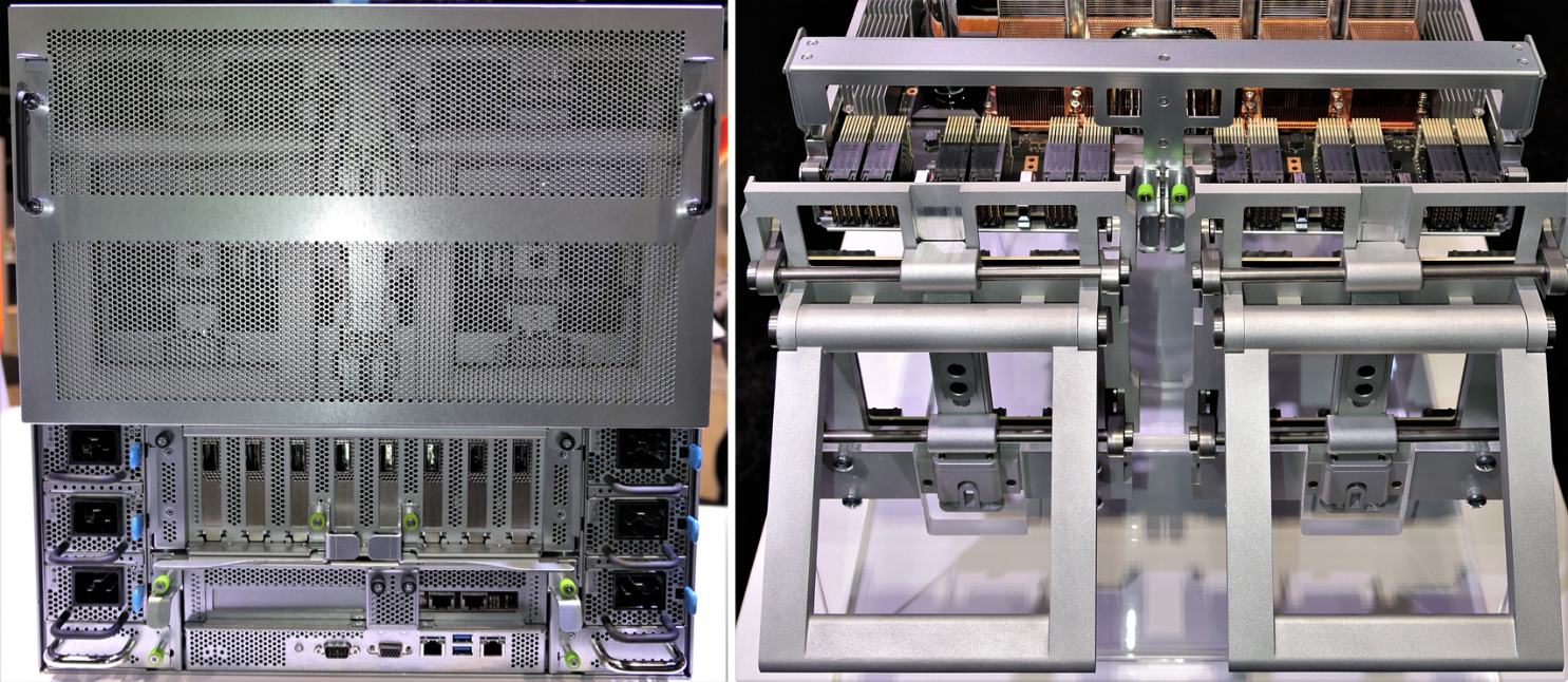
The giant latches are visible behind the electrical shielding panel on the back of an assembled DGX-2 and quite prominent on the exploded physical demo.
Without the huge latches on the back of the chassis, even these guys might not be able to service the chassis and close it back up:

The Server Part
The actual server node inside the DGX-2 is a high-end dual-processor Intel Xeon Platinum system with 1.5 TB of system memory and dual 10/25 Gb/sec Ethernet ports. It seems strange to say that a large memory dual-processor Xeon Platinum server is the least special part of the design, but there we are.
Combining 1.5 TB system memory with the 512 GB of GPU shared memory give the overall system a total of 2 TB of memory addressable by all the compute elements in the DGX-2 chassis.
Power Consumption
The DGX-2 consumes 10 kilowatts. It houses six 2 kilowatt power supply units (PSU) in a “5+1” configuration. If one PSU fails, the single spare is substituted for the failed PSU, which can then be replaced.
It is worth noting that Nvidia increased the power consumption rating for the new Tesla V100 32 GB SXM3 module to 350 watts from the 16 GB version’s 300 watt rating. Nvidia also upgraded the 32 GB version’s air-cooled heat sink.
Given that each GPU board has eight GPUs and six NVSwitch chips, it is likely that each GPU board consumes about a third of the overall system power budget, probably in the 3.6kW ballpark.
This also gives us an interesting handle on HBM power consumption. Doing the simple math, it appears that 16 GB of V100 HBM has a TDP of 50 watts (17 percent of 300 watts), so 32 GB would be 100 watts (29 percent of 350 watts). This seems like a reasonable power consumption trade-off for much better performance and much larger datasets.
Commentary
We expect that Nvidia will eventually sell NVSwitch chips to its system manufacturer customer base. NVSwitch is an integral part of NVLink 2.0 system enablement for any system implementing more than four GPUs in the highest performance configurations possible. It will therefore become indispensable for both high-performance computing (HPC) and AI training applications.
Also, IBM integrated NVLink 2.0 into its Power9 chips. A system designer can opt to design-in a socket for an IBM Power9 processor wherever you see a “GPU” in the above interconnect topologies. The upshot for IBM is that IBM and the OpenPower community can create NVLink 2.0 system designs that do not need the overlay PCI-Express 3.0 x16 switches, which simplifies server designs, improves performance, reduces the size of GPU accelerated servers, lowers costs, and reduces power consumption.
We would very much like to see an NVSwitch-enabled IBM Power9 system design. Two IBM Power9 processors with six Nvidia Tesla V100 32 GB GPUs connected by six NVSwitch chips is the right ratio for a very nice next-generation version of IBM’s “Newell” Power Systems AC922 machine.
Paul Teich is an incorrigible technologist and a principal analyst at TIRIAS Research, covering clouds, data analysis, the Internet of Things and at-scale user experience. He is also a contributor to Forbes/Tech. Teich was previously CTO and senior analyst for Moor Insights & Strategy. For three decades, Teich immersed himself in IT design, development and marketing, including two decades at AMD in product marketing and management roles, finishing as a Marketing Fellow. Paul holds 12 US patents and earned a BSCS from Texas A&M and an MS in Technology Commercialization from the University of Texas McCombs School.

Inside Tesla’s Innovative And Homegrown “Dojo” AI Supercomputer
How expensive and difficult does hyperscale-class AI training have to be for a maker of self-driving electric cars to take a side excursion to spend how many hundreds of millions of dollars to go off and create its own AI supercomputer from scratch? And how egotistical and sure would the …

Datacenter Becomes Nvidia’s Largest Business
Something that we have been waiting for a decade and a half to see has just happened: The datacenter is now the biggest business at Nvidia. Bigger even than the gaming business for which it was founded almost three decades ago. The rise of the datacenter business has been no …
Nvidia Picks Up The Pace For Datacenter Roadmaps
Heaven forbid that we take a few days of downtime. When we were not looking – and forcing ourselves to not look at any IT news because we have other things going on – that is the moment when Nvidia decides to put out a financial presentation that embeds a …
come on Nvidia.. you own Mellanox now.. you putting 25gb ports in? mellanox can do 80gbit no probs