
How expensive and difficult does hyperscale-class AI training have to be for a maker of self-driving electric cars to take a side excursion to spend how many hundreds of millions of dollars to go off and create its own AI supercomputer from scratch? And how egotistical and sure would the company’s founder have to be to put together a team that could do it?
Like many questions, when you ask these precisely, they tend to answer themselves. And what is clear is that Elon Musk, founder of both SpaceX and Tesla as well as a co-founder of the OpenAI consortium, doesn’t have time – or money – to waste on science projects.
Just like the superpowers of the world underestimated the amount of computing power it would take to fully simulate a nuclear missile and its explosion, perhaps the makers of self-driving cars are coming to the realization that teaching a car to drive itself in a complex world that is always changing is going to take a lot more supercomputing. And once you reconcile yourself to that, then you start from scratch and build the right machine to do this specific job.
That, in a nutshell, is what Tesla’s Project Dojo chip, interconnect, and supercomputer effort is all about.
At the Hot Chips 34 conference, the chip, system, and software engineers who worked on the Dojo supercomputer unveiled many of the architectural features of the machine for the first time, and promised to talk about the performance of the Dojo system at the Tesla AI Day 2 event on September 30.
Emil Talpes, who worked at AMD for nearly 17 years on various Opteron processors as well as on the ill-fated “K12” Arm server chip, gave the presentation on the Dojo processor that his team created. Debjit Das Sarma, who was a CPU architect at AMD for nearly as long, was credited on the presentation and is currently the autopilot hardware architect at Tesla, as was Douglas Williams, about whom we know nothing. Bill Chang, principal system engineer at the car maker, spent a decade and a half at IBM Microelectronics designing IP blocks and working on manufacturing processes before helping Apple move off of X86 processors to its own Arm chips, and Rajiv Kurian, who has been working at Tesla and then Waymo on autonomous car platforms, talked about how the Dojo system. As far as we know, Ganesh Venkataramanan, who spoke at Tesla AI Day 1 last August and who is senior director of autopilot hardware at Tesla, is in charge of the Dojo project. Venkataramanan was also a leader on the CPU design teams at AMD for nearly a decade and a half.
So in a weird way, Dojo represents an alternate AI future that might have been at AMD had Tesla come to it to help design a custom AI supercomputer from scratch, from the vector and integer units inside a brand new core cores all the way out to a full exascale system designed for scale and ease of programming for the AI training use case.
Like a number of other relatively new platforms from AI startups, the Dojo design is elegant and thorough. And what is most striking are the things that Tesla’s engineers threw out as they focused on scale.
“The defining goal of our application is scalability,” Talpes explained at the end of his presentation. “We have de-emphasized several mechanisms that you find in typical CPUs, like coherency, virtual memory, and global lookup directories just because these mechanisms do not scale very well when we scale up to a very large system. Instead, we have relied on a very fast and very distributed SRAM storage throughout the mesh. And this is backed by an order of magnitude higher speed of interconnect than what you find in a typical distributed system.”
And with that, let’s dive into the Dojo architecture.
The Dojo core has an integer unit that borrows some instructions from the RISC-V architecture, according to Talpes, and has a whole bunch of additional instructions that Tesla created itself. The vector math unit was “mostly implemented” by Tesla from scratch, and Talpes did not elaborate on what this means. He did add that this custom instruction set was optimized for running machine learning kernels, which we take to mean that it would not do a very good job running Crysis.
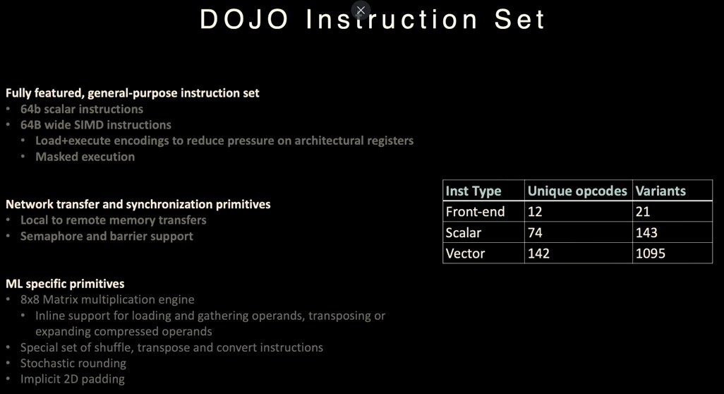
The Dojo instruction set supports 64-bit scalar instructions and 64 B SIMD instructions, and it includes primitives to deal with transferring data from local memory to remote memories and has support for semaphore and barrier constraints, which is necessary to get memory operations in line with instructions running not just within a D1 core, but across collections of D1 cores. As for the ML-specific instructions, there are a set of shuffle, transpose, and convert instructions that are commonly done in software that are now etched in transistors, and the core also does stochastic rounding and can do implicit 2D padding, something that is commonly done by adding zeros to both sides of a piece of data to tweak a tensor.
What Talpes did make clear is that the D1 processor, the first in what we presumably be a line of Dojo chips and systems, is a “high throughput, general purpose CPU” and that it is not an accelerator as such. Or more precisely, Dojo is architected to accelerate itself and not have some outboard device do it.
Each Dojo node has a single core, and is a full-fledged computer with a CPU dedicated memory and I/O interfaces. This is an important distinction because each and every core can do its own thing and is not dependent on shared caches or register files or anything.
The D1 is a superscalar core, which means it supports instruction-level parallelism within its core, like most chips do these days, and it even has a multi-threaded design to drive more instructions through that core. But the multithreading is more about doing more work per clock than having isolated threads that can run separate instances of Linux as a virtual machine, and therefore the Dojo implementation of simultaneous multithreading (SMT) does not have virtual memory, has limited protection mechanisms, and the Dojo software stack and applications manages the parceling out of chip resources.
The D1 core is a 64-bit processor and has a 32 B fetch window that can hold up to eight instructions; an eight-wide decoder can handle two threads per cycle. This front end feeds into a four-wide scalar scheduler that has four-way SMT, which has two integer units, two address units, and a register file for each thread. There is a two-side vector scheduler with four-way SMT as well, which feeds into a 64 B wide SIMD unit or into four 8x8x4 matrix multiplication units.
Each D1 core has a 1.25 MB SRAM that is its main memory. It is not a cache, and if anything, the DDR4 memory that hangs off of the larger Dojo network (more about this in a second) is treated more like bulk storage than anything else. That SRAM can load at 400 GB/sec and store at 270 GB/sec, and the chip has explicit instructions to move data to or from external SRAM memories of other cores in the Dojo machine. Embedded in that SRAM are a list parser engine that feeds into the pair of decoders and a gather engine that feeds into the vector register file, which together can dispatch information to or take information from other nodes without a bunch of additional operations as is common with other CPU architectures.
This list parsing function is one of the key features unique to the Dojo chip design:
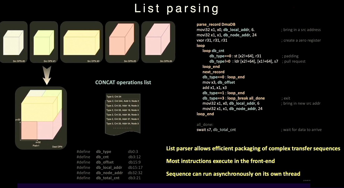
This is essentially a way to package up different bits of data so it can be transferred efficiently between the D1 cores in a system.
The D1 core supports a slew of data formats. The scalar unit supports integers with 8, 16, 32, or 64 bits, and that vector unit and its associated matrix units support a wide variety of data formats, with a mix of precisions and numerical ranges, and quite a few of them are dynamically composable by the Dojo compiler. Look at this and weep, GPU makers:
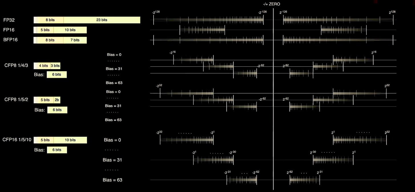
Talpes noted that FP32 formats have more precision and more range than many parts of AI training applications need, the FP16 format specified by the IEEE does not have enough range to cover all layers of processing in a neural network; conversely, the Bfloat format create by the Google Brain team has a wider range, but less precision. And so Tesla has come up not just with an 8-bit FP8 format for lower precision and yet higher throughput vector processing, but a set of configurable 8-bit and 16-bit formats where the Dojo compiler can slide around the precision of the mantissas and exponents as shown in the chart above to cover a wider set of ranges and precisions. At any given time, up to 16 different vector formats can be used, but each 64 B packet has to be of the same type.
On the upper right of the diagram, you will see the network on chip router, which links multiple cores together into a 2D mesh. The NOC can handle eight packets across the node boundary, 64 B in each direction, with every clock cycle, which is one packet in and one packet out in all four directions to each core’s nearest neighbor in the mesh. That router also can do one 64 B read from and one 64 B write to the local SRAM each cycle, so data can be moved between cores.
With all of that etching done on the D1 core, which is done in a 7 nanometer process from foundry partner Taiwan Semiconductor Manufacturing Co (like there was another option), Tesla gets out the cookie cutter and just starts replicating D1 cores and interlinking them on the mesh, like this:
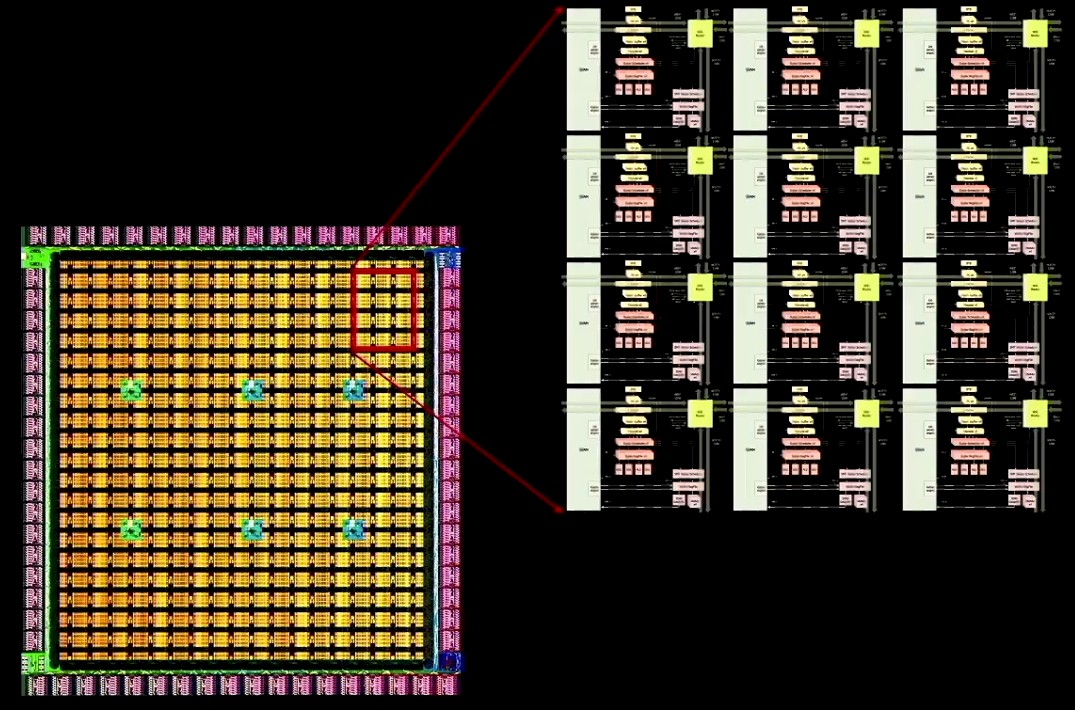
A dozen of the D1 cores are arranged into a local block, and a 2D array of 18 cores by 20 cores is created, but for some reason only 354 D1 cores are available. The D1 die runs at 2 GHz and has a total of 440 MB of SRAM across those cores, and delivers 376 teraflops at BF16 or CFP8 and 22 teraflops at FP32. There is no FP64 support in the vector units. So many HPC workloads won’t run on this D1 chip and neither will some AI applications that do make use of 64-bit vector math. Tesla doesn’t need to care – it just needs to run its own AI applications, and if it wants to add FP64 support on the D2 or D3 chip to run its HPC simulation and modeling workloads for so Musk’s companies can design spaceships and cars, well, that is fairly easy after all of this work has been done.
The D1 die has 576 bi-directional channels of SerDes wrapped around the die to link to other D1 dies, and 8 TB/sec of bandwidth across all four edges of the D1 die. The dies, which weigh in at 645 square millimeters, are made to seamlessly connect through those SerDes into what Tesla calls a Dojo training tile. Like this:
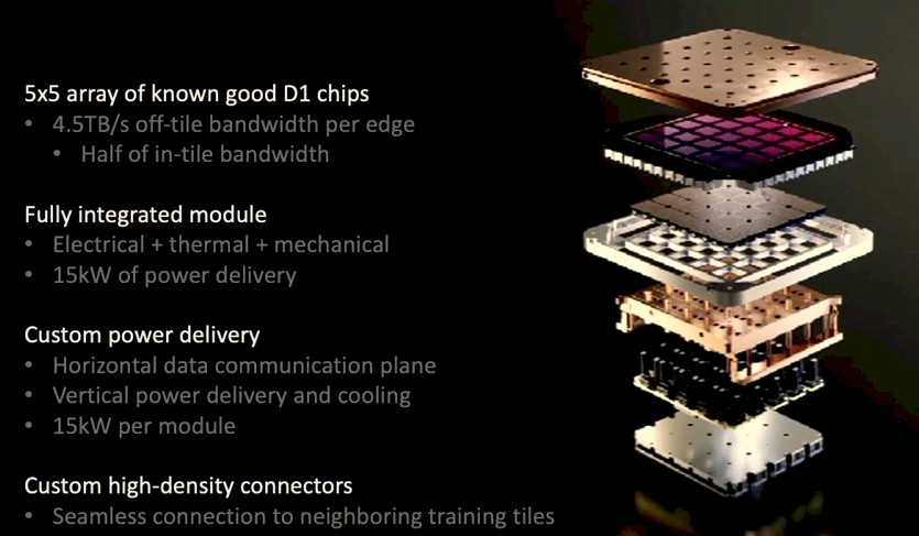
The training tile takes 25 known good D1 dies and packages them up into a 5×5 array, interlinked. The outside edge of the training tile has 36 TB/sec of aggregate bandwidth implemented on 40 I/O chips; that is half of the bi-sectional bandwidth of the meshes of 2D meshes across the D1 chips inside the tile. The tile has 10 TB/sec of on-tile bi-sectional bandwidth, and 11 GB of SRAM memory across the cores. Each tile delivers 9 petaflops of BF16/CFP8 oomph.
Those Dojo training tiles consume 15 kilowatts, and are obviously going to be water cooled, and they are designed so that multiple training tiles can be interconnected to neighboring tiles. It is not clear how this happens, but clearly you will want a long row of interlinked tiles, oriented either horizontally or vertically, and not separate racks with trays of a few devices that then need some sort of optical or electrical cable of enormous proportions and tanglement to carry the data between the tiles. Vertically works, like this:
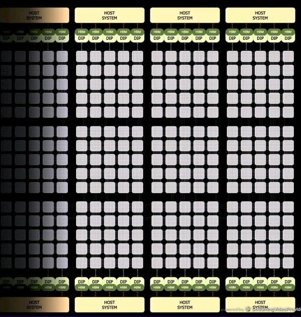
You will note in the diagram above that there are what are called Dojo Interface Processors, or DIPs, on the edges of the D1 mesh, and these are hooked into the D1 mesh as well as host systems that power the DIPs and perform various system management functions. Each training tile has a total of 11 GB of private SRAM main memory, but the system needs some sort of larger memory that sits reasonably close to the mesh. In this case, Tesla has chosen to create a DIP memory and I/O co-processor that packs 32 GB of shared HBM memory – we don’t know what kind yet, but it is either HBM2e or HBM3 – as well as Ethernet interfaces to the outside world as well as to do more direct hopping between tiles and cores than is possible through this gigantic mesh. The picture shows a pair of hosts has ten of these DIPs installed, for a total of 320 GB of HBM memory for each set of three Dojo training tiles. But the wording on the chart says there is 160 GB allocated to every tile, which means one host per tile, not two hosts for three tiles as shown here.

That DIP card has two I/O processors with two banks of HBM memory each, and the card supplies 32 GB of HBM memory with 800 GB/sec of bandwidth. That looks like a slightly geared down HBM2e memory to us. The card implements the Tesla Transport Protocol (TTP), a proprietary interconnect that smells like CXL or OpenCAPI to us, over PCI-Express to deliver full DRAM memory bandwidth into the Dojo training tile. At the other end of the card, there is a 50 GB/sec TTP protocol link running atop an Ethernet NIC, which connects out to stock Ethernet switches, which is either a single 400 Gb/sec port or a paired set of 200 Gb/sec ports. The DIP plugs into a PCI-Express 4.0 x16 slot that delivers 32 GB/sec of bandwidth per card. With five cards per tile edge, there is 160 GB/sec of bandwidth going into the host servers and 4.5 TB/sec going from the HBM2e memory to the tile.
As we pointed out already, the DIPs are not just implementing DRAM as a fat local storage, but also are providing another dimension of networking that can be used to bypass the 2D mesh when it would take a lot of hops to get across all of those cores and tiles. Like this:

To got end to end across the 2D mesh across the system might take 30 hops, according to Chang, but using the TTO over Ethernet protocol and a fat tree Ethernet switch network, it only take four hops. The bandwidth is a lot lower, obviously, but the latency is a lot lower across that third dimension (hence Z plane) of networking.
The Dojo V1 Training Matrix is the base system that Tesla is building, and it has six training tiles, 20 DIPs across four host servers, and a bunch of adjunct servers linked into the Ethernet switch fabric, like this:
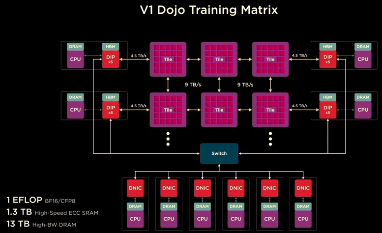
The base Dojo V1 system has 53,100 D1 cores, is rated at 1 exaflops at BF16 and CFP8 formats, and has 1.3 TB of SRAM memory on the tiles and 13 TB of HBM2e memory on the DIPs. The full-on Dojo ExaPod system will have 120 tiles in total, and will have 1,062,000 usable D1 cores, weighing in at 20 exaflops.
Heaven only knows what it cost to research, develop, and manufacture the machine and its software stack. At the moment, tesla is getting the Dojo chips back from the foundry and is testing them in its lab. Presumably it will be able to build the machine soon. If that was not the case, tesla would not have brought it up at all. No timing was given for then the complete system would be available.
By the way, this thing runs PyTorch. Nothing as low level as C or C++, nothing remotely like CUDA. And the other neat thing about the Dojo machine is that that SRAM presents itself as a single address space. It is one flat memory area with local compute hanging off of the chunks of its memory.
We look forward to seeing how Dojo does on AI benchmark tests. Let it loose.

The Edge Propels HPE While Datacenter Taps The Brakes
Customers of Hewlett Packard Enterprise have one foot on the gas and one foot on the brakes at the same time that the company is transitioning from selling gear outright to customers to selling them subscriptions that spread the cost – and therefore HPE’s recognized revenues – out over time. …
Talking AI Costs And Addressable Markets With SambaNova
The only way to accurately predict the future is to live it, but just the same, prognostication is one of the things that we humans love to do. It helped us stay alive all of these millennia, presumably because we are right more than wrong when we run scenarios in …

Pushing The Limits Of HPC And AI Is Becoming A Sustainability Headache
As Moore’s law continues to slow, delivering more powerful HPC and AI clusters means building larger, more power hungry facilities. “If you want more performance, you need to buy more hardware, and that means a bigger system; that means more energy dissipation and more cooling demand,” University of Utah professor …
Dojo will accelerate current development of FSD – no starting from scratch.
Also Dojo is not build specifically for autonomous driving – it’s generally specialized for training neural networks including FSD, Optimus bot or anything including AWS-like outsourcing.
During the Q&A it was stated that Tesla have silicone of the chip in their lab, not that they have a supercomputer up and running. And what state that silicone is currently in was not even addressed. The “Base Dojo V1 system” does not exist yet, is nowhere near deployment, and you got suckered into writing this fluff piece in present tense because you didn’t do your due diligence as a journalist. Also, Musk did not found Tesla; this has comprehensively been disproven time and time again.
Wake up on the wrong side of the bed this morning?
First, it is silicon.
Second, you’re right. The system is not yet built. I was talking about the architecture. And yes, I should have been more clear about that. And I will fix that.
As for you, the world doesn’t need your hostility. It generates enough already.
Have a good day.
pretty short sighted. it’s in production now. who cares if he founded it or not, he’s making it kick ass now.
Ironic that Dojo is doing so well and seemingly has so much promise when Tesla felt the recent need to upgrade their A100 GPU count: “Tesla has boosted its in-house AI supercomputer with thousands of additional Nvidia A100 GPUs. The Tesla supercomputer had 5,760 A100 GPUs about a year ago, and that count has since risen to 7,360 A100 GPUs — that’s an additional 1,600 GPUs, or about a 28% increase.” tomshardware(dot)com/news/tesla-brags-about-in-house-supercomputer-now-with-7360-a100-gpus
That’s now. Also, that GPU cluster may be used for lots of things, including CAD/CAE/CFD. As I pointed out, Dojo can’t really do that — yet.
Hi Timothy
Thanks for the article.
Someone in the comments section of the most recent ‘Tesla Daily’ YouTube video has asked a curious question. Googling has left me suspecting the answer is almost definitely Fremont / San Jose / Santa Clara, but I haven’t seen explicit information.
The question is:Where is DOJO being built and assembled? Where is it going to be located when fully functional?
Can you help?
Thanks,
Anthony