
Marvell has had a large and profitable I/O and networking silicon business for a long time, but with the acquisitions of Inphi in October 2020 and of Innovium in August 2021, the company is building a credible networking stack that can take on Broadcom, Cisco Systems, and Nvidia for the $1.3 billion or so in switch chips sold into the datacenter each year, which is growing at about 15 percent a year to more than $2 billion by 2026.
The rise of Marvell among the hyperscalers and cloud builders has made it unattractive for Intel to stay in the switch ASIC market with the Barefoot Networks “Tofino” family of programmable switch chips, which it just put out to pasture in January as part of its huge cost-cutting maneuvers.
Everyone makes their choices in an intensively competitive datacenter silicon market, and even Marvell, which acquired Arm server chip maker Cavium back in November 2017 and then mothballed its “Triton” ThunderX3 line in the summer of 2020, has had to make some tough choices.
With Amazon Web Services making its own Graviton Arm server chips and Ampere Computing coming out aggressively with a chip designed more for cloud builders and hyperscalers, and AMD aggressively broadening its Epyc X86 server chip line with many-core designs starting with “Bergamo” Epycs and Intel following suit with “Sierra Forest” Xeon XPs, Marvell was prescient (or had good competitive intelligence) and backed out of ThunderX – although if you want to license it to do a custom part, Marvell would love to talk to you.
Cavium itself was no slouch in Ethernet switching for the datacenter, and had acquired programmable switch chip pioneer XPliant in July 2014 and then bought Fibre Channel and Ethernet switch ASIC and network adapter chip business from QLogic in June 2016. XPliant never had much in the way of sales, although Arista Networks did launch some switches based on XPliant’s XP80 chip back in 2016. Cisco Systems made Nexus switches based on Barefoot Networks Tofino ASICs as well as on Innovium Teralynx ASICs.
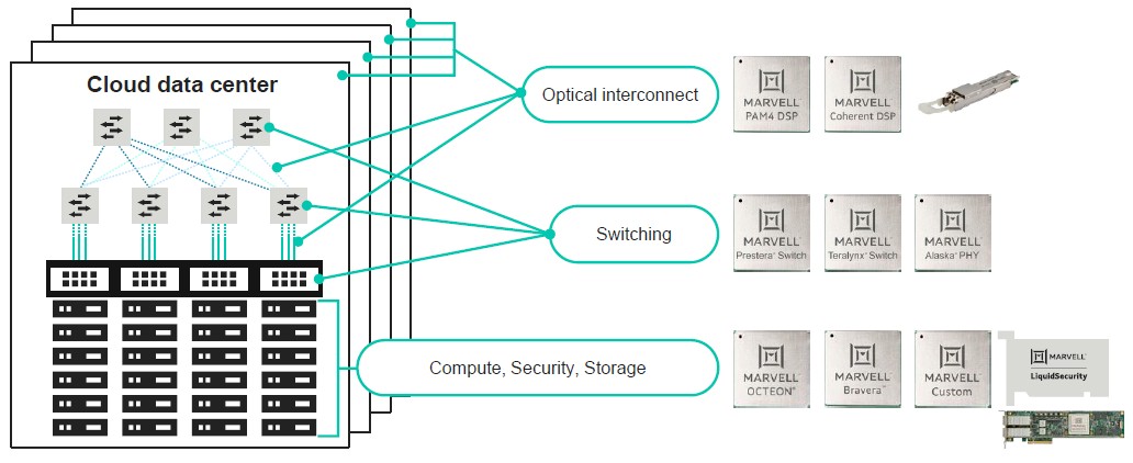
Marvell wants networking more than it wants server compute, and has its own Prestera Ethernet switch ASIC line, which it still sells, and it got the Xpliant line by virtue of the Cavium deal, too. But the acquisitions of Innovium and Inphi gave Marvell the chips that are of interest to the hyperscalers and cloud builders and also made those chips part of the portfolio of a large, trusted, multifaceted, and profitable corporation, thereby making it safe for these large datacenter operators to choose Innovium and Inphi chips.
It is in all of that context that Marvell has announced the 51.2 Tb/sec Teralynx 10 ASIC for 800 Gb/sec switches and the 1.6 Tb/sec Nova PAM-4 digital signal processor that will drive future Ethernet modules with native 200 Gb/sec signaling per lane (after encoding overhead is taken off, of course).
By the way, in the wake of the Innovium acquisition, Marvell said it was going to rebrand the Teralynx line to Prestera 9X and keep its own chips as the Prestera 2X line, but that has not happened. Teralynx still is its own brand, and Teralynx 10 is going to be one of the first 51.2 Tb/sec ASICs in the field to further drive the 800 Gb/sec Ethernet wave that is just a ripple right now.
From 1 Tb/sec to 51.2 Tb/sec
Innovium was founded nine years ago and dropped out of stealth mode in March 2017 with its Teralynx 7 switch chip, which scaled from 2 Tb/sec to 12.8 Tb/sec across its SKUs and aimed mostly at all tiers of the network for hyperscalers and cloud builders. Two years later, chasing top of rack and edge switching use cases, Innovium launched the Teralynx 5 chip in September 2019 spanning from 1 Tb/sec to 6.4 Tb/sec and using the same 50 Gb/sec PAM-4 SerDes that were employed in the Teralynx 7. Taking on Broadcom’s “Tomahawk 4” StrataXGS, Innovium launched the Teralynx 8 switch chips in May 2020, aiming at leaf, spine, and datacenter interconnect (DCI) use cases at the hyperscalers and cloud builders and spanning from 8 Tb/sec to 25.6 Tb/sec using 100 Gb/sec PAM-4 encoding on the lanes that are bundled together to create an Ethernet port at a given bandwidth.
To date, Innovium and now Marvell has shipped more than 5 million Teralynx ports at 400 Gb/sec equivalent speeds into some of the biggest datacenters in the world.
The Teralynx 10 is a bigger, fatter switch ASIC that is also based on 100 Gb/sec SerDes with PAM-4 encoding, and according to Nariman Yousefi, executive vice president of the Automotive, Coherent DSP, and Switch Group at Marvell, the 100 Gb/sec SerDes used in the Teralynx 10 chip was designed by the combined Marvell, Inphi, and Innovium teams, much as Nvidia took its SerDes team and created a new-and-improved set of signaling circuits for the 800 Gb/sec Spectrum-4 Ethernet chips announced in April 2022. And the Marvell and Inphi teams really know their SerDes, according to Yousefi, and heavily contributed to that design.
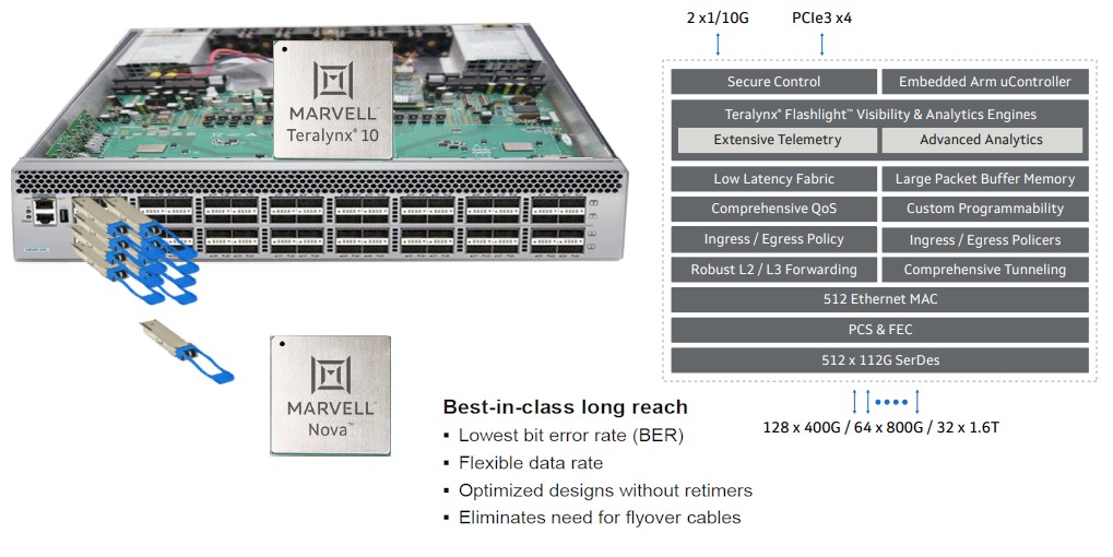
As is the case with all of the 100 Gb/sec PAM-4 encodings used in the switch business, the native speed of the lanes on the SerDes is 50 GHz, and the PAM-4 encoding allows for two bits per signal to be transmitted, which gives an effective speed of 100 GHz and therefore 100 Gb/sec.
As is usually the case with switch ASICs these days, no one gives out die shots or a lot of feeds and speeds, but we can tell you that Teralynx 10 has 512 of these SerDes and that the die is monolithic and not comprised of chiplets. It is etched using 5 nanometer processes from Taiwan Semiconductor Manufacturing Co, as is the Nova PAM-4 DSP we will talk about in a minute.
“I can’t tell you exactly what the die size is for Teralynx 10, but I can tell you that if you call up TSMC and ask what its reticle limit is for 5 nanometers, that is the size of our chip,” jokes Yousefi.
The Teralynx 10 can drive 128 ports at 400 Gb/sec, 64 ports at 800 Gb/sec, and 32 ports at 1.6 Tb/sec, all of which still sounds a bit like the future to us here at The Next Platform. Ther is a second version of the Teralynx 10 that has only half of its SerDes activated, which delivers up to 25.6 Tb/sec of aggregate switching capacity. Here are some sample configurations of the Teralynx 10 ASICs and port types, form factors, and port counts:
For the 51.2 Tb/sec Teralynx 10:
- 1U: 32 x 1.6T (OSFP-XD)
- 2U: 64 x 800G (OSFP or QSFP-DD800)
For the 25.6 Tb/sec Teralynx 10:
- 2U: 64 x 400G (QSFP-DD or OSFP)
- 1U: 32 x 800G (OSFP or QSFP-DD800)
- 4U: 128 x 200G (QSFP56)
You can drive higher radix out of these switches at lower bandwidth by using breakout cables, of course. This eliminates tiers in the network, reducing cost and in many cases latency across the network, too. Ports can be geared down to run at 25 Gb/sec, 50 Gb/sec, or 100 Gb/sec natively as well so the network and the servers do not have to be upgraded in unison.
The Teralynx 10 is back from the foundry and will be sampling to prospective customers in the second quarter of 2023. If the past is any indication, that means customers will have Teralynx 10 switches in the field within nine to twelve months after that first sampling, and we strongly suspect that many of those building switches using this ASIC will be using the SONiC/SAI open source networking stack or their own custom network operating system atop the devices.
One of the things that the Marvell team is most proud of, and that the Teralynx 10 chip is benefitting from, is what Yousefi calls the lowest bit error rate in the industry. He does not provide specifics, but say that competitive Ethernet switches (presumably from Broadcom and Nvidia) of the prior generation had a latency that was, on average, 1.7X higher than with the Teralynx 7 ASIC and that this delta between the Teralynx 10 and its 51.2 Tb/sec competitors will be maintained.
“The trick is to achieve best-in-class bit error rates given a high loss channel at a very good power draw,” says Yousefi. “And that is where Marvell has put in a tremendous amount of research and development. The important thing is that the same technology that goes into the Teralynx 10 PAM-4 SerDes goes into the Nova PAM-4 DSPs. Now they don’t need retimers or complicated switch boards – you can just connect our chips together.”
Inphi and now Marvell has been aggressive on that 2X performance cadence every two years, and that is because that is what the hyperscalers and the cloud builders expect. Like this:
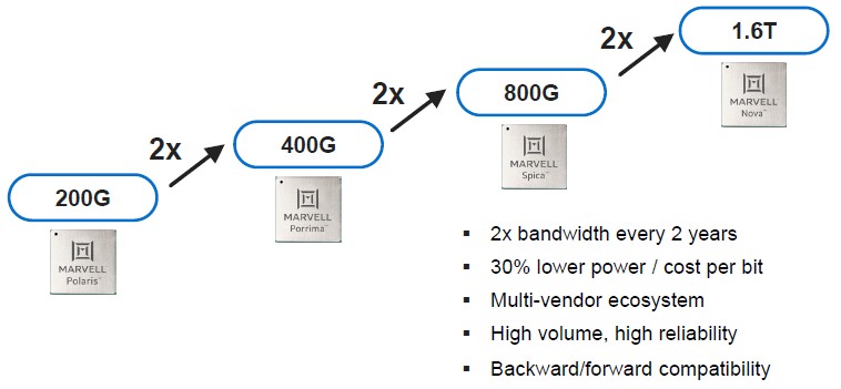
Those Nova DSPs are the fourth generation of such DSPs based on PAM-4 technology, with the prior three – Polaris, Porrima, and Spica – coming from Inphi before the acquisition. With each generation Inphi and Marvell have been able to drive higher speeds per wavelength (denoted by lambda, or λ) which drives cost per bit down by 30 percent, drives power consumption down by 30 percent, and because there are half the number of modules for any given bandwidth, the optics used are therefore twice as reliable because there are half as many that can potentially fail.
But perhaps more important for the hyperscalers is the fact that they like 32 port leaf switches that fit in a 1U form factor, and with the 200 Gb/sec per lambda signaling, that means you can do that with 1.6 Tb/sec ports. For the same bandwidth running with 100 Gb/sec per lambda signaling, you need 64 ports and it takes up 2U of rack space. The Nova DSPs are therefore essential for the adoption of 51.2 Tb/sec switch ASICs at the hyperscalers and cloud builders.
The Nova DSP chips are sampling now.

Looking Ahead To Marvell’s Future ThunderX Processors
If you are going to take on Intel in server processors, you have to play the same kind of long game that Intel itself played as it jumped from the desktop to the datacenter. And now that Cavium is part of chip giant Marvell and others have exited the field …
The Future Of AI Training Demands Optical Interconnects
Artificial intelligence has taken the datacenter by storm, and it is forcing companies to rethink the balance between compute, storage, and networking. Or more precisely, it has thrown the balance of these three as the datacenter has evolved to know it completely out of whack. It is as if all …
Marvell Adds Hyperscale Ethernet With Innovium Acquisition
Cash used to be king, and now market capitalization is. That’s one of the reasons that the biggest players in the semiconductor arena are snapping up competitors, startups, and suppliers in adjacent chip markets at an increasing pace and with very large bags of “money.” Stock isn’t quite bitcoin, which …
Be the first to comment