

Say what you will, but among the many vendors that have tried to break into the datacenter with Arm server chips, Marvell, by virtue of the hard work done by Cavium, which it acquired, and Broadcom, which sold its “Vulcan” design to Cavium when it exited the business, has been the most successful in terms of shipments and ecosystem. And with the “Triton” ThunderX3, Marvell is bringing its first ground-up processor design – being done by the combination of the former Cavium and Broadcom Arm server chip teams with a healthy dose of its own engineers – to market later this year.
We did an in-depth preview of the Triton chip back in March, but there were still a lot of details that were not known at the time. Some of these details were filled in this week during the Hot Chips conference by Rabin Sugumar, chief architect of the ThunderX line of chips.
Back in March, we were told that the ThunderX3 was a monolithic design and, furthermore, that it would not have 64 cores as we had been anticipating but would scale all the way up to 96 cores. All of these statements are true – mostly.
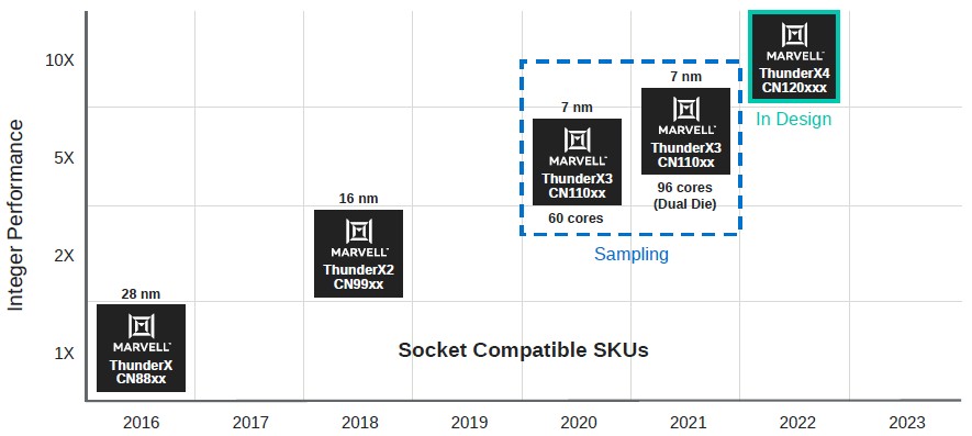
As it turns out and as you can see from the roadmap above, one flavor of the ThunderX3 chip will have 60 cores and another will scale to 96 cores – but that latter chip is a dual-chip module, or DCM. It is not clear how many cores the single-chip modules, or SCMs, will have, and Sugumar did not elaborate but only talked about the number of active cores on the SCM and the DCM, which top out at 60 cores and 96 cores, respectively.
Here is the block diagram that Sugumar showed off for the 60 core variant of the Triton chip, which apparently has the custom Marvell cores in a 60 by 10 array bleeding out over top of the DDR4 memory controllers on the chip. This is not meant to be taken literally, of course.
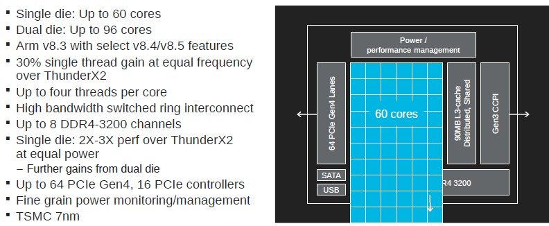
What we want to know is the absolute number of physical cores on the SCM die, and even though we suspect that it is probably more like 64 cores per SCM, there is no reason why it can’t be a grid such as that shown in the block diagram above. We like things to be in multiples of two when it comes to systems, which 60 certainly is, but we like powers of two better. But if you look at this L3 cache ring interconnect diagram closely that Sugumar showed, you can get the answer:
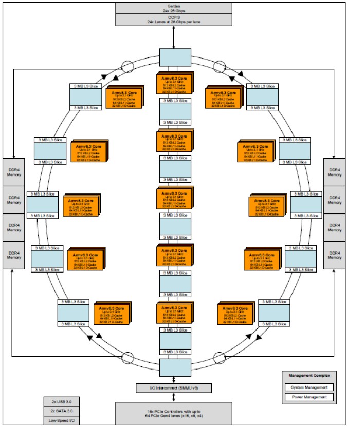
If you look very closely at this, the orange Armv8 core blocks are stacked four deep, and there are 15 of those orange locks spread out across those interlocking rings that comprise the L3 cache bus. That’s 60 cores, no extras to help improve yield and no dark silicon embedded in the design. The 96-core DCM is a pair of these chips, but with only 48 cores each activated and another 12 cores per die that are either all duds or a mix of latent and dud. What is clear, then, is that Marvell could, in theory, scale the ThunderX3 up to 120 cores if the thermal limits would allow it, and could probably significantly increase the throughput of its top bin DCM parts at some point in the future by turning on some or all of those latent 24 cores – provided that the yield on the 7 nanometer processes from foundry partner Taiwan Semiconductor Manufacturing Corp is good enough, of course.
As we have previously reported, the ThunderX3 chip uses a custom Marvell Armv8.3 core with four-way simultaneous multithreading that also pulls in features of the Armv8.4 and Armv8.5 specs. The way that threading is implemented, each thread has a full copy of the architecture state of the core, but they share execution units, pipeline resources, cache hierarchy, and core interfaces. As far as the operating system running on top of ThunderX3 will see four distinct CPUs for each thread, or 240 threads (and 240 “cores”) per socket on the SCM. By the way, the addition of SMT to the architecture adds only about 5 percent to the transistor count and die area. So this is a good tradeoff, Marvell thinks. For encoding work, the SMT delivers about 1.28X more oomph running across four threads instead of one, and on MySQL databases, it is more like 2.21X more oomph. Mileage varies with SMT, of course, depending on the nature of the software.
The updated Triton core will have 30 percent better performance at the same frequency as the Vulcan core used in the ThunderX2. The chip has eight DDR4 memory controllers that top out at 3.2 GHz speeds, which is a tiny bit faster than the 3.1 GHz speed that the ring diagram above shows for the Arm cores. The 60 core chip also has 90 MB of distributed and shared L3 cache, which is implemented on the ring in a pair of 3 MB slices that are near each group of four Arm cores but which do not have affinity to any particular core as is the case in some processor designs. The ring has an I/O interconnect, and sixteen PCI-Express 4.0 controllers, each with four lanes, yield a total of 64 lanes coming out of the processor sockets. There are also two USB 3.0 ports and two SATA 3.0 ports plus some other low-speed I/O ports that come off the southbridge, and there is also 24 lanes of I/O running at 28 Gb/sec that implement the third generation of the Cavium Coherent Processor Interconnect (CCPI3), which creates NUMA links between sockets. As far as we know, ThunderX3 only supports two-way NUMA systems, later in the presentation, Sugumar said that the snoop filters in the snoop-based coherence only supported one or two sockets. So that’s that. (We were hoping Marvell would step up to four sockets.) To make the DCM, we suspect that half of the lanes in each chip are burned to make the interconnect between the chips in the socket and the other half are used to connect across a pair of sockets. In a sense, this is a four-socket machine, and it will be interesting to see the topology that Marvell uses to link two DCMs together.
If you look carefully at that diagram, it shows four interconnected rings, with two switches that allow data to find the closest path between any two cache segments and core groups. (This is a bit like the tram at some international airports.) Sugumar said that Marvell didn’t think that it was necessary to move to a mesh interconnect with this generation of ThunderX processors, but we strongly suspect that it will move to a mesh interconnect as other CPU designers have done with the ThunderX4 chips due in 2022. As it is, the improved switched ring interconnect in ThunderX3 was sufficient to help drive memory bandwidth, as gauged by the STREAM Triad benchmark, up by 15 percent per core compared to ThunderX2.
Here is the block diagram of the Triton core:
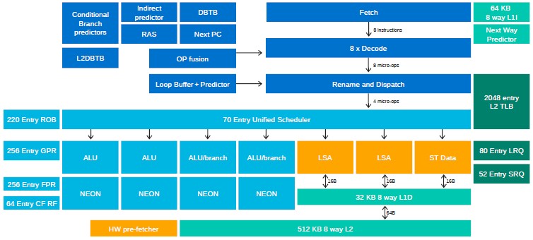
Each core has 64 KB of L1 instruction cache and 32 KB of L1 data cache, plus a 512 KB L2 cache that spans all four of the arithmetic logic units (ALUs) and all four of the 128-bit Neon SIMD units. What those SIMD units do not have is support for the Scalable Vector Extensions (SVE) super-wide bit-busy vectors that Fujitsu implemented in its A64FX Arm server processor, but Sugumar hinted strongly that support for SVE would be coming in ThunderX4.
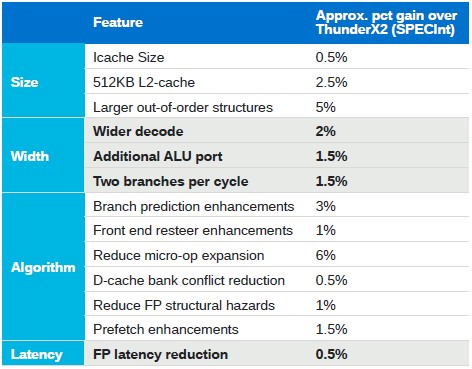
Here is a neat little chart that Sugumar put up that showed the contribution that each major element that was tweaked for ThunderX3 contributed to SPEC integer performance:
And here, speaking very generally, is how Marvell thinks the ThunderX3 will stand up to the ThunderX2 in terms of raw performance:
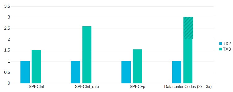
Datacenter codes means things like Java middleware or MySQL databases.
The Triton ThunderX3 processors, in both the 60 core SCM and the 96 core DCM, are sampling now. As we have said in the past, Marvell’s plan is to ship variants with 32, 36, 40, 48, 54, 60, and 96 cores; we suspect that there could eventually be variants with 72 cores and 84 cores as well, although these have not been mentioned.

Can Marvell Profit As It Tries To Triple Its Business By 2028?
A rising tide may lift all boats, and that is a good thing these days with any company that has an AI oar in the water. But the question is will any of that water be potable – by which we mean profitable. Thus far, depending on how cynical you …
The Future Of AI Training Demands Optical Interconnects
Artificial intelligence has taken the datacenter by storm, and it is forcing companies to rethink the balance between compute, storage, and networking. Or more precisely, it has thrown the balance of these three as the datacenter has evolved to know it completely out of whack. It is as if all …

Marvell Pivots To AI Silicon, Looks Poised To Profit
It is hard to bet against the GenAI boom, and thus far it is also hard for anyone other than Nvidia to profit from it. No one knows these facts better than Marvell Technology, who along with rival chip maker Broadcom, is seeking to benefit from the bevy of custom …
The architecture information, performance claims are great. In fact, I almost vouch for the performance claims and the $/performance of TX3 snd it’s feasibility.
Having worked on TX2 extensively, esp. for HPC and having written a detailed piece on TNP of the “Arm Ecosystem”, I am confident that TX3 is a very good architecture as well as will deliver on the performance.
What I am worried about, is about their execution –
1) How many customers does Marvell have for TX2?
2) Apart from Astra, what’s the biggest deployment of TX2 among cloud and hyper-scalars?
3) What is Marvell’s strategy to execute on TX3 market adoption?
4) Is TX3 targeted at Hyperscalars or HPC or both?
5) Who is leading TX3 esp. after Gopal Hegde has left Marvell, and a slew of departures from the ThunderX team?
6)