
When Globalfoundries decided to stop its development and rollout of both immersion lithography and extreme ultraviolet (EUV) lithography at the 7 nanometer process node back in August, it looked as if IBM, second only to AMD as a server chip customer for its most advanced fab in Malta, New York, would be left in a lurch with its future Power processors.
But that was never really the case anymore than with AMD, which is switching from Globalfoundries to Taiwan Semiconductor Manufacturing Corp for its next-generation “Rome” Epyc processors. As we suspected, IBM did not go with TSMC, as most server, networking, and custom ASIC chip makers do in the datacenter arena these days, but rather chose long-time chip research and development partner Samsung as its wafer baker.
We said at the time that you didn’t exactly need a supercomputer running machine learning inference to figure this out. Big Blue stopped being its own fab four years ago when it paid Globalfoundries $1.5 billion to take IBM Microelectronics off its hands. At that time, IBM also committed itself to the former AMD in-house foundry to take over its own foundry on East Fishkill, New York to continue making Power8 and Power8’ chips based on 22 nanometer processes that were developed by IBM and continued by Globalfoundries. That East Fishkill foundry was in the process of being converted over from 45 nanometer equipment and processes that were used to make the Power7 chip from 2010 and also from the 32 nanometer processes that were used to make the Power7+ in 2012.
(By the way, that is a prime sign there and it designates a change in the I/O and possibly memory subsystems in a Power processor; it is distinct from a plus sign, which means a change in process or architecture or both in a Power chip, but well short of a major version which has big changes.) Globalfoundries also took over the manufacturing of IBM’s System z mainframe processors, which have some common elements with the Power chip line but which have a distinct instruction set and memory and I/O architecture from the Power line.
Significantly, the Power chip roadmap that we discovered in August 2015 and that IBM talked more specifically about in early 2018 called for Globalfoundries to make IBM’s future Power10 processor, which have a very good chance of being installed in at least one and possibly two exascale-class supercomputer systems in the United States in the 2021 to 2022 timeframe.
The expectation back in 2015 was that the Power10 chip would be made using 10 nanometer processes at Globalfoundries, not 7 nanometer transistor gate geometries. Take a look:
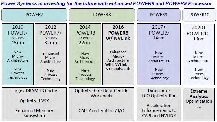
This particular roadmap above was not public at the time we wrote about it. Earlier this year at the OpenPower Summit, IBM put out a roadmap that offered more insight into what salient characteristics across the Power7 through Power10 were important as a hint of how the architecture of the processors and systems would change:
You will notice that the Power10 column only promises a “new microarchitecture” and a “new technology” and does not give a precise dimension for the processes used to make the transistors. It says neither 10 nanometers nor 7 nanometers, and we think it is because IBM did not have high confidence in the yields with the 7 nanometer process node (despite the two-pronged approach that Fab8 in Malta was using to get to 7 nanometers one way or the other) or the commitment from other chip designers to use Globalfoundries at either the 10 nanometer node, which was scrapped in favor of going all-in on 7 nanometers at some point in the past few years.
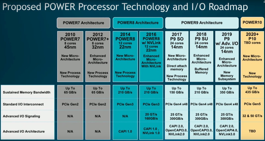
The original deal between IBM and Globalfoundries was to run from 2014 through 2024 and on out to the 10 nanometer node. This is one of the reasons why Big Blue paid $1.5 billion to get IBM Microelectronics out of its revenue stream and, with a $4.7 billion writeoff back in 2014 for its fabs in Vermont and New York, out of its books. But the deal only made it through five years, if you count the Power9’ processor update that is coming in 2019 based on a refined 14 nanometer processors from Globalfoundries. The Power9’ is expected to have enhancements to the I/O and memory circuits, much as the follow-on Power8’ added NVLink support to the Power8 design.
In some roadmaps we have seen, IBM was going to double up the cores on Power10 to 48 per monolithic die using 10 nanometer processes sometime between 2019 and 2020 and then move to 7 nanometers to get even more cores on the die by Power11 out beyond that. The chip manufacturing nodes are getting harder for every server chip maker, and it is wreaking havoc on the roadmaps.
The choice of Samsung was an obvious one. Samsung is the largest semiconductor manufacturing company in the world – larger even than Intel – and it makes its own Arm processors for smartphones, tablets, and other embedded devices, and even flirted with the idea of making Arm server chips at some point. Samsung has engaged with IBM in a chip manufacturing and design partnership for the past 15 years, and some notable achievements were the first deployment of high-k/metal gate transistors in foundry manufacturing way back in 2008, initially for 32 nanometer processes, which is one of the reasons that this process was able to deliver around 35 percent more performance and between 30 percent and 50 percent power reduction over 45 nanometer processes of the time. Back in July 2015, IBM, Globalfoundries, and Samsung worked together through the chip research center at the State University of New York’s Polytechnic Institute to demonstrate a 7 nanometer goosed by silicon germanium channel transistors and using EUV lithography that could, in theory, cram 20 billion transistors on a single die.
Samsung has no choice but to invest in wafer baking techniques and the foundries that implement them – just like Intel – because Taiwan Semiconductor Manufacturing Corp, the only other fab working on 7 nanometer manufacturing and the clear winner thus far in the fab race, cannot absorb the volumes of either Intel or Samsung. Samsung is using EUV lithography to get to 7 nanometers, and TSMC is doing 7 nanometer initially with conventional water immersion lithography to start but pretty rapidly moving to EUV, which should be in production in early 2020 by Samsung.
“We expect that we will go into the market as we originally planned in late 2021 or early 2022 with our 7 nanometer product family,” Bob Picciano, senior vice president in charge of IBM’s Cognitive Systems division, tells The Next Platform. “That remains unchanged, and we are able to maintain our roadmap and keep the schedules our customers are expecting. We know Samsung really well across some different spaces, and this gives Samsung a good opportunity to build out a new competency in the foundry business.”
By the way, the next generation IBM mainframe processor, presumably called the z15, will be using the same updated 14 nanometer process from Globalfoundries that is being used on the Power9’ chip, and then the successor z16 processor for mainframes will be based on the same 7 nanometer processes from Samsung that the Power10 chip will use.

IBM Bets Big On Native Inference With Big Iron
Everyone knows that machine learning inference is going to be a big deal for commercial applications in the years ahead, but no one is precisely sure how much inference is going to be needed. There is, however, an increasing consensus that for enterprise customers – as distinct from hyperscalers, cloud …

Big Blue Open Sources The Core Inside BlueGene/Q Supercomputers
Earlier this month, we were talking to the James Kulina, the new executive director of the OpenPower Foundation, which is the organization created by IBM and Google back in the summer of 2013 to create a community around the Power architecture. IBM had already open sourced the Power instruction set …
Can IBM Get Back Into HPC With Power10?
The “Cirrus” Power10 processor from IBM, which we codenamed for Big Blue because it refused to do it publicly and because we understand the value of a synonym here at The Next Platform, shipped last September in the “Denali” Power E1080 big iron NUMA machine. And today, the rest of …
“At that time, IBM also committed itself to the former AMD in-house foundry to take over its own foundry on East Fishkill, New York to continue making Power8 and Power8’ chips based on 14 nanometer processes that were co-developed by IBM and Globalfoundries.”
Power8 and 8NV are 22nm.