

Earlier this month, we were talking to the James Kulina, the new executive director of the OpenPower Foundation, which is the organization created by IBM and Google back in the summer of 2013 to create a community around the Power architecture. IBM had already open sourced the Power instruction set last summer, and Kulina, who has spent his career in the open source software ecosystem, said it was only logical that at some point he would ask IBM to open source an actual Power core so people could get a leg up on designing Power-based chips.
And here we are, not even a month later, and IBM is open sourcing the VHDL files for one of its Power cores and donating it to the OpenPower community.
That was fast, at least by the standards of the hardware business. But in fact, opening up Power cores – and we think there will be others – is something that has been in the works for some time, according to Mendy Furmanek, president of the OpenPower Foundation and the person at IBM in charge of Power processor verification and open hardware business development.
“There are actually several reasons why the Power-A2 core was picked as the first core to be opened up,” Furmanek tells The Next Platform. “The first is that people have been asking us to do it. Also, the Power-EN and the Power-A2 that followed it were developed to be optimized for throughout but also for customization. The design has auxiliary units that can be tightly coupled to the core. We were almost ahead of our time a decade ago, since this is exactly what everybody is doing with their special purpose designs and we were also creating an edge of network chip. And on top of that, the Power-A2 design has the ability to balance performance and power.”
Some history of the Power-EN and Power-A2 is perhaps in order to parse this a bit, and to explain why IBM didn’t just grab the Power8 or Power9 core used in its own commercial chips and lob the VHDL files out onto GitHub and call it mission accomplished.
Big Blue’s Systems and Technology Group, which created its chippery and servers, and its IBM Research arm worked together on a massively parallel, low power Power variant called the Wire-Speed Processor specifically designed to run high throughput jobs that would normally be relegated to switch chips or other kinds of network ASICs, but also run heavily threaded workloads like databases or – as it turns out – HPC simulations and models really well, too.
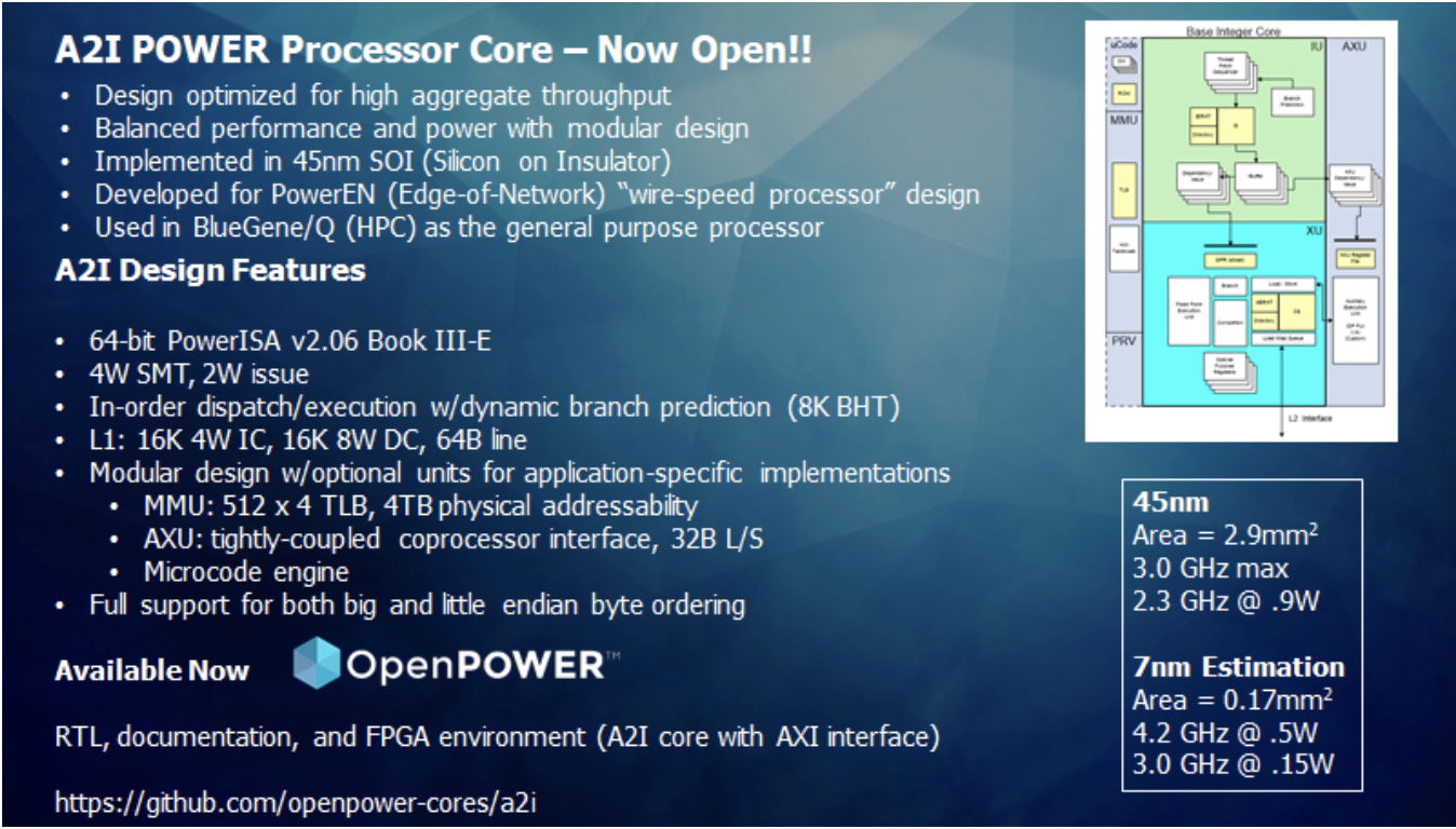
This test chip, eventually called the Power-EN, short for edge of network, was developed using IBM’s own 45 nanometer silicon-on insulator (SOI) chip making techniques, which were world class a decade ago when this was unveiled. (In February 2010, to be precise.) The Power-EN had 16 cores, with 64-bit processing and memory addressing, running at a base clock speed of 2.3 GHz and a clock ceiling of 3 GHz; it supported simultaneous multithreading with four threads per core. The cores were arranged in blocks of four with a shared L2 cache weighing in at 2 MB and etched using IBM’s embedded DRAM (eDRAM) technology, which has been used in Power server chips for generations to great effect. Each core had 16 KB of L1 instruction cache and 16 KB of L1 data cache. The chip had 1.43 billion transistors, which was a decent count for a decade ago, which included two DDR3 memory controllers (with one or two DIMMs per channel), three chip-to-chip links for implementing NUMA memory sharing in a node (with 20 GB/sec of bandwidth per link, which was a lot at the time), four 10 Gb/sec Ethernet controllers, and two PCI-Express 2.0 controllers. The Power-EN had integrated cryptographic and compression accelerators, and also included a special Ethernet host adapter that could also act as a packet processor. It supported server virtualization hypervisors and could virtualize its own I/O and storage.

The concept of the Wire-Speed Processor was to merge network processing and database and application and business logic processing – all heavily threaded and all dependent on getting data from outside sources as part of an application stack.
Interestingly, the Power-EN core (which was called A2) was an in-order, rather than an out-of-order, executor, and could issue two instructions per clock. And even more interestingly in hindsight – wait for it – the Power-EN had the only modern processor cores that we have heard of that did not have speculative execution in its circuits. Speculative execution has hit all commercial processors with the Spectre and Meltdown security vulnerabilities that Google revealed in January 2018 in varying degrees, but this is not a concern with those using the Power-EN’s A2 core.
Like, for instance, the BlueGene/Q massively parallel supercomputers that were installed at Lawrence Livermore National Laboratory and Argonne National Laboratory in the United States and Forschungszenrum Julich in Germany, just to name three examples. The BlueGene/Q machine, as it turns out, used a modified version of the Power-EN processor called the Power-A2, which we wrote about way back from the Hot Chips conference in 2010.
The Power-A2 processor had a total of 18 cores on the die: 16 of them were used for compute, one was used to run a Linux operating system and to keep the jitter off the other cores, and the final one was a spare that was really used to increase the yield on the chip as it came out of the IBM fabs. (You put an extra one in there you know you are going to lose, and you can use more of the chips that come off the line.)
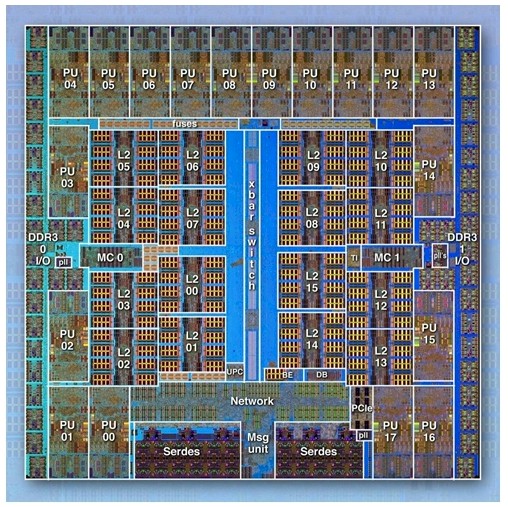
In this case, IBM embedded the 5D torus interconnect used for the BlueGene/Q system on the die, which had 11 links running at 2 GB/sec. The Power-A2 had a 14-port crossbar switch/router at the center of the chip to support point-to-point, collective, and barrier messages. It also implemented direct memory access between nodes. The Power-A2 chip used in BlueGene/Q had 1.47 billion transistors and ran at a mere 1.6 GHz to keep the thermals at a low 55 watts. It took 96 racks of machines with 1.57 million cores to reach 20 petaflops of performance in the “Sequoia” system at Lawrence Livermore, but it was done in 6.6 megawatts, which was, again, pretty good for the time.
There is one more reason why the core at the heart of the BlueGene/Q is the first one to be open sourced: IBM had the FPGA emulator for the chip all ready to go, and could carve out the core and give it to the OpenPower community. IBM has a lot of homegrown tooling that it has used to develop its chips, and this is not something it can let loose on the community – any more than Google could have just taken its Borg container and system orchestrator and dropped it on GitHub. It had to scrub it down, rewrite it in Go and for a more general purpose set of use cases, and call it Kubernetes.
The Power-A2 core supports both big endian and little endian byte ordering, which means it can run IBM’s own AIX and IBM i operating systems as well as Linux swinging either way (which it does on Power). It would be very interesting to see someone make some truly scale-out Power chips for running these operating systems; the 24-core Power9 and presumably 48-core Power10 have very heavy cores in them and are not designed for power efficiency, but rather beastly throughout and scale up.
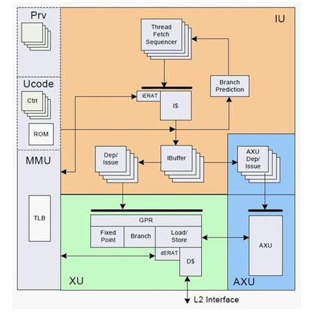
Here is the zoom on that block diagram for that integer core, since it is a bit fuzzy:
As far as we know, IBM is not opening up the quad-pumped floating point unit that was part of the Power-A2 chip and that gave BlueGene/Q all of its petaflops. And it is important to realize as well that IBM is opening up the A2I core, not the full Power-A2 chip.
Here’s the fun bit. Implemented in 45 nanometers, the Power-A2 integer core was 2.9 square millimeters in area and generated 0.9 watts at 2.3 GHz. Projecting out to 7 nanometer processes (presumably implemented at Samsung, IBM’s current fab partner for Power chips), this area will drop to 0.17 square millimeters for the integer core and power will be 0.15 watts at the base 3 GHz and 0.5 watts at the top speed of 4.2 GHz.
In addition to opening up the Power-A2 core, IBM is getting requests to open up other cores and chips, including some of its older 32-bit designs, believe it or not. People are also interested in getting the game console chips IBM created for Sony and Microsoft opened up – we think the “Cell” variant of the Power line, famously used in the “Roadrunner” supercomputer at Los Alamos National Laboratory from 2009 to 2013, would be interesting to play around with, too.
And there is always a chance that Power8, Power9, or even Power10 could be opened up at the core or even fully. Anything is possible. We have suggested – and Furmanek did not say this was stupid but she also made no commitments – that Power10 should be the last chip that IBM designs by itself and that Power11 should be the first one that involves a community of chip designers all helping out. This would be very hard to do, we think, sort of like building an elephant by committee. But there should be a way to get a more varied Power chip line created than what IBM is delivering today, and opening up the core on the Power-A2 is a good second step. The PowerISA being open was never enough, but was also a good first step.

For IBM, AI Inference Is The Most Important HPC
All of the commercial platform creators in the world, since the dawn of time, which arguably started in the enterprise in April 1964 with the advent of the System/360 mainframe, wants the same things. They want to create a flexible, integrated, and useful system where data can be stored and …
Bending The Supercomputing Cost Curve Down
One of the recurring themes at the recent HPC Day event that we hosted ahead of the SC19 supercomputing conference in Denver was that capability class supercomputers are getting more and more expensive. While it is good that these machines can be deployed to run two different kinds of workloads …
Big Iron Will Always Drive Big Spending
Starting way back in the late 1980s, when Sun Microsystems was on the rise in the datacenter and Hewlett Packard was its main rival in Unix-based systems, market forces compelled IBM to finally and forcefully field its own open systems machines to combat Sun, HP, and others behind the Unix …
bluegeneQ was tbe leader for many years in the Green500 list. It was the only homogeniuous architecture in the top of that list before accelerators+technology cached up. Releasing A2 is great as it provides a very effcient and scalable core for free!
Hi Tim,
Thanks for the article, as a former BG/Q admin it’s interesting to see this move by IBM, wonder if anything will come of it.
One minor nit, on a standard production IBM BG/Q these compute nodes ran IBM’s Compute Node Linux which was a cut down OS kernel (no fork() nor execve() for instance) written in a mix of C & C++ and licensed under the Eclipse Public License. Also they had no I/O capabilities other than forwarding any I/O to be done off to the air-cooled I/O nodes which did run a modified Linux kernel and RHEL6.
All the best,
Chris
Oops – brain fail in previous comment – “Compute Node Linux” was meant to be “Compute Node Kernel”. It’s late here!