

Everyone knows that machine learning inference is going to be a big deal for commercial applications in the years ahead, but no one is precisely sure how much inference is going to be needed. There is, however, an increasing consensus that for enterprise customers – as distinct from hyperscalers, cloud builders, and HPC centers – the proper place to do such inference is not only inside of the skins of their back-end servers where their databases and applications run, but literally on the CPU itself.
There are good reasons for this, and it is one reason why we think Nvidia is able and willing to pay $40 billion to acquire Arm Holdings, the company that controls the Arm architecture. If inference stays largely native on CPUs at enterprises and is fairly modest as a share of the compute in the system, then Nvidia needs a piece of that action because it won’t be offloaded to GPUs that are designed for a much heavier workload and that may deliver excellent price/performance on inference but not are as cheap as a few billion transistors on a CPU die and that can never offer the low latency and absolute security that an on-chip accelerator can. If you never leave the server CPU memory space, there is a lot less auditing and compliance to worry about.
This is why all of the server CPU makers who matter are adding some sort of matrix math acceleration – more than just having a vector engine – to their chips. They are not doing this for their amusement, but because their enterprise customers, who had to deal with outboard encryption and decryption PCI-Express cards for many years, are telling them they don’t want that. They want AI inference to be native, fast, and simple, invoked with some instructions like any other kind of on-chip accelerator. They don’t want to learn CUDA or ROCm or oneAPI to use it, either.
Intel, which is still the world’s largest and most profitable server CPU maker by a long shot – and it is very important to remember that – has been tweaking its vector math units to do mixed precision integer and floating point math to support inference, and is taking it up another notch with the forthcoming “Sapphire Rapids” Xeon SP processors and their Advanced Matrix Extension (AMX) matrix math accelerator. The Zen 3 core in the AMD “Milan” Epyc processors have a pair of 256-bit AVX2-compatible vector units that can do mixed precision integer and floating point instructions for inference. The Neoverse “Zeus” V1 and “Perseus” N2 cores from Arm Holdings have a pair of 256-bit and 128-bit Scalable Vector Engine (SVE) math units, respectively, that can do the same mixed precision math for inference. And finally, on the upcoming Power10 chip, due in a couple of weeks from IBM, each core has eight 256-bit vector math engines that support FP64, FP32, FP16, and Bfloat16 operations and four 512-bit matrix math engines that support INT4, INT8, and INT16 operations; these units can accumulate operations in FP64, FP32, and INT32 modes.
With the “Telum” z16 processor being unveiled today by IBM at the Hot Chips 33 conference, which will be used in its System z mainframe systems, Big Blue is taking a different approach to accelerating inference. Rather than gut the z15 processor and add mixed precision integer and floating point math, the company instead picked up the third generation of AI Core inference accelerators developed by IBM Research and plunked it down into the z16 processor and then tightly integrated it with the z architecture instruction set to expose it as a native function.
Take a look at the Telum z16 chip, which is named after the javelin that the Greek goddess Artemis used to hunt when she wasn’t in the mood to shoot her bow (see the big iron metaphor there?), which has 22.5 billion transistors, and which is a much more streamlined design than the z14 and z15 chips that preceded it:
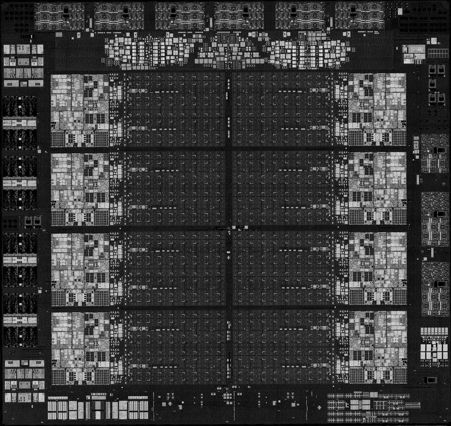
The eight z16 cores and their L2 caches are connected by a double ring with 320 GB/sec of bandwidth both ways. The L2 caches dominate the center of the chips, as you can see, and weigh in at a mere 32 MB, replacing great gobs of L3 cache on the prior CPUs and L4 caches that were on the NUMA interconnect chipsets used with the previous two generations of mainframe processors. IBM is also apparently making a smaller System z processor with the z16 to take better advantage of the 7 nanometer shrink with new foundry partner Samsung – with only eight cores – and probably significantly ramping up the yield on the chips relative to what it would be if IBM tried to put sixteen cores on a single die to boost per socket performance. IBM is making up the difference by putting two eight-core chips into a single socket, linked by a proprietary interconnect that tightly coupled the chips into what looks like a monolithic chip to the operating systems (z/OS, Linux, and VM are the important ones) and that only eats two clock cycles to jump from chip to chip.
The contrast in architecture between the z15 and the z16 is striking. Look at the z15 chip:
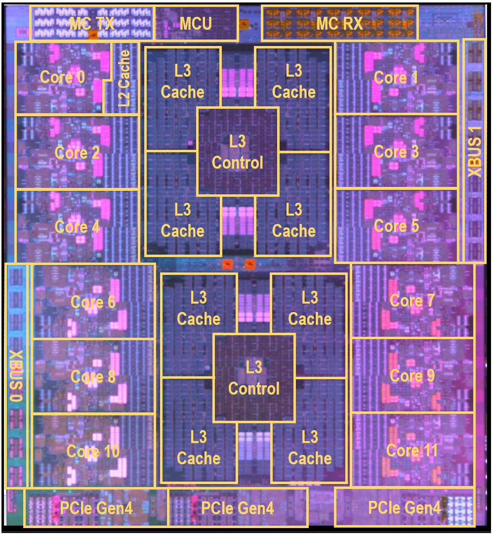
The z15 chip was implemented in 14 nanometer processes at GlobalFoundries and had 8 MB of L2 cache per core (half for data and half for instructions) across its twelve cores. Each core had 256 KB of L1 cache (again, half for data and half for instructions). In the very center of the chip was an L3 cache complex with two L3 controllers and eight L3 cache blocks at 32 MB each that looked like a unified L3 cache at 256 MB. The top-end System z machine had five drawers of four-socket processors, with some of them being used for compute and come of them being used for system I/O processors – what IBM called CPs and SPs. Each drawer had one of the L4 cache/interconnect chips in it, which looked like this:
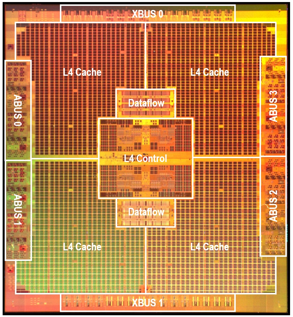
The Xbus ports on the z15 provided the NUMA links between processors in a single drawer and the ABus ports on the L4 cache/interconnect chip were used to link the drawers together. Each of these interconnect chips had 960 MB of L4 cache, which fed into the L3 caches and were a lot quicker than main memory and hugely faster than flash memory in the compute complex.
And while we always admired all of this hierarchy, for its novelty as much as its effectiveness in creating a huge I/O monster processor, Christian Jacobi, the chief architect of IBM’s z processors, started from scratch with the z16 design and just chucked it all in the garbage to come up with a more streamlined design that would deliver linear scalability not only for traditional transaction processing and batch processing workloads, but also deliver scalable AI inference performance at very low latency. And, we presume, require fewer chips in the system and lower cost chips to boot.
With the z16, IBM is doing away with physical L3 and L4 caches, Jacobi tells The Next Platform, and is implementing L2 caches that can be made to look like a shared L3 or L4 cache as necessary. (We have never seen this approach before, but it is very likely needed to maintain compatibility with the z14 and z15 machines, which expect dedicated L3 and L4 caches.)
Gone are the NUMA interconnect chips, too. Now, the z16 has a dual-chip module (DCM) interface logic block, which is on the center and right portion at the bottom of the chip in the picture of the z16 above. There is a logic block at the top that implements the on-drawn XBus interconnects (as well as the overall fabric control) and a relatively small cross-draw ABus interconnect chip on the right side of the chip above the two DDR5 memory controllers. The z16 system is very tightly coupled now, like this:
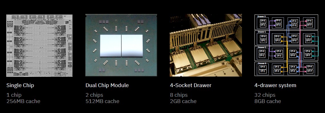
The pair of z16 chips are paired up in the DCM package and look like a 16-core chip with 512 MB of L2 cache, partitionable as L3 and L4 cache as needed. Four of these sockets are put in a drawer and tightly coupled with the XBus interconnects and four of these drawers are linked to each other using he ABus interconnects into a compute complex with 32 chips and 8 GB of L2 cache. Importantly, the interconnect is a flat topology, with all chips interconnected. No more CPs and SPs. The I/O is handled by a pair of PCI-Express 5.0 controllers, which are on the left side, top and bottom. This looks very much like a Power7, Power8, Power9, and we presume a Power10 NUMA topology.
For the record, the Telum processor will run at a base clock rate of more than 5 GHz and has a die that is 530 square millimeters. (The z15 ran at 5.2 GHz.) By contrast, the Power10 chip has twice as many cores in SMT8 mode and four times as many cores in SMT4 mode, with one of the cores held back to improve yields; it is slightly larger at 602 square millimeters but has slightly fewer circuits at 18 billion transistors. The z16 core only supports SMT2 multithreading, by the way. So the fatness of its cores has more to do with registers and branch tables and other things that make a fast and deep pipeline work well.
On the lower left of the Telum z16 chip, the logic block that is about a third of the area, just to the left of the DCM interface, is the AI Accelerator. This is the neat bit of this architecture, and gives us some insight into how much inference enterprise customers and IBM’s architects, working together, think they really need to embed inference in their workloads.
Let’s take a look at this AI Accelerator:
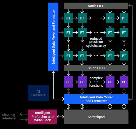
There are two bits to this accelerator. There is a collection of 128 processor tiles (PTs in the chart) hooked together into an array that supports FP16 matrix math (and its mixed precision variants) on multiply-accumulate floating point units. This was designed explicitly to support the matrix math and convolutions of machine learning – including not just inference but low precision training, which IBM expects might happen on enterprise platforms. The AI Accelerator also has 32 complex function (CF) tiles, which support FP16 and FP32 SIMD instructions and are optimized for activation functions and complex operations such as RELU, Sigmoid, tanh, log, high-efficiency SoftMax, LSTM, and GRU functions.
A prefetcher and write-back unit hooks into the processor and L2 cache ring interconnect, and also links into a scratchpad that in turn links to the AI cores through a data mover and formatting unit, which as the name suggests formats data so it can be run through the matrix math unit to do its inferencing and yield the result. The pre-fetcher can read data out of the scratchpad at more than 120 GB/sec and can store data into the scratchpad at more than 80 GB/sec; the data mover can pull data into and push data from the PT and CF cores in the AI unit at 600 GB/sec, or about a third of the aggregate bandwidth of a GPU accelerator card these days. But it is linked directly to the CPU cores through the ring bus and it will have a hell of a lot less latency than going out over the PCI-Express bus to an external GPU or FPGA to do inference.
This low latency and lack of complexity in terms of the programming model is the whole point of getting AI inference onto the CPU complex.
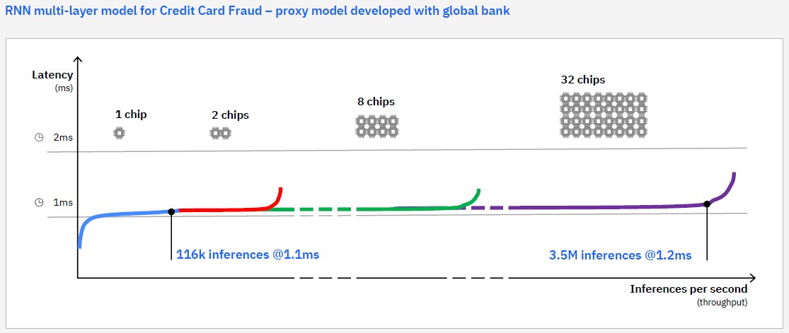
In the above chart, IBM has simulated the performance of a credit card fraud application that is running at one of its global banking customers and uses a multi-level recurrent neural network. As you can see, scaling this application from one chip to two in a DCM to eight in a drawer to 32 in a system is pretty linear in terms of both performance and latency. Somewhere between 1.1 milliseconds and 1.2 milliseconds is a very, very good latency for a real-world application to do its inference. These systems will be doing tens of thousands of transactions per second and will need to be doing a lot of inferencing to take fraud detection up another notch.
“We will be moving from fraud detection to fraud protection,” explains Ross Mauri, general manager of the System z division within IBM Systems group.
And just in case you are wondering why we care about the Telum z16 chip, it is not just because we like system architecture, although that is certainly part of it. IBM sells z machines as Linux-only machines under the LinuxOne brand, and he z15 machine with 190 “customer configurable cores,” meaning the CPs not the SPs, was able to support 2.4 million Docker containers doing real work on a mixed workload simultaneously. At the time it launched in September 2019, IBM said that was 2.3X the number of containers that an X86 cluster could do. Specifically, IBM compared Linux running on two z15 cores against a two-socket Xeon SP-6140 Gold server, both running NGINX. That’s two cores on the mainframe versus 36 cores on the X86 server, but remember, some of those X86 cores have to do I/O and network. If you do the math, that would be about 218 X86 servers with a pair of those Xeon SP chips each. Move up to Ice Lake, and it might be something closer to 200 machines.
Fully, loaded, the System z16 fully loaded will support 256 cores, which will have a little more oomph per core. (IBM said the z16 socket would have 40 percent more performance than the z15 socket, and if you do the math, the IPC on the z16 core is up maybe 7 percent.) In any event, by this logic, a z16 box with 256 cores should be able to handle about 3.5 million Docker containers. If you move the X86 server from Skylake to Ice Lake and keep it at 18 cores per socket, it would take 190 machines to handle the original 2.4 million Docker containers and it would take about 275 to deliver the 3.5 million Docker containers that we expect the full-on z16 machine to deliver.
We don’t expect for hyperscalers to move to mainframes given this, because the costs don’t warrant such a move. But we absolutely do expect for the mainframe shops that run the banks, insurance companies, and governments of the world to keep their mainframes. And that means IBM has a future, and it has money to invest in other things, such as the Power line that does attach AI and HPC more directly.

The Difficulty – And Necessity – Of Parsing Out AI Spending
For a decade before the generative AI boom took off in late 2022, classical artificial intelligence, used for all kinds of self-learning predictive algorithms, was destined to be a very large component of the IT stack at most organizations in the world. With all of the excitement around GenAI, it …
IBM’s AI Accelerator: This Had Better Not Be Just A Science Project
Big Blue was one of the system designers that caught the accelerator bug early and declared rather emphatically that, over the long haul, all kinds of high performance computing would have some sort of acceleration. Meaning, some kind of specialized ASIC to which a CPU would offload its math homework. …
TSMC Can’t Be Caught Or Bought, Only Sought Or Stolen
It is not hard to figure out who is in the catbird seat in the semiconductor foundry business. In 2024, according to CC Wei, chief executive officer of Taiwan Semiconductor Manufacturing Co, the overall industry, including making chip masks, etching logic wafers, and packing and testing finished chips, grew by …
Is this AI Core Inference Accelerator the logical successor/descendant of the PS3 Cell SPE?
https://www.psdevwiki.com/ps3/CELL_BE
It is certainly one of the “logical” successors–to a certain extent the matrix math units on the Power10 are too. But it may not be a literal successor.
The cache approach is nothing new. I wrote about it in my Cache Memory Book in 1993. See Page 154.
In those days it was called Direct Data Intervention.
It’s still cool!
And, like all aspects of cache design, it takes massive brainpower to figure out what you want to do, and then a trivial amount of logic to actually implement it!
Thanks for a great review of the architecture.
Will there be OMI DIMM RAIM?