

It has been more than a decade since Intel fielded its first credible processors aimed at four-socket machines, and it is no coincidence that makers of RISC and Itanium systems that used to enjoy high revenues and margins on big iron systems have been in decline since that time. The top-end Xeon E7 processors offer the same class of resiliency and stability as those venerable processors, and often at a much lower price point.
With the launch of the “Haswell-EX” Xeon E7 v3 processors, Intel is turning the heat up a little more on its competitors, who are making their cases for their Power and Sparc motors and the systems that use them.
The Xeon E7 v3 processors were designed to work in the current “Brickland” server platforms, which debuted with the “Ivy Bridge-EX” Xeon E7 v2 processors back in February 2014. This Brickland platform will also support the future “Broadwell-EX” processor, presumably due in a year or so. High-end servers are not exactly being a high volume product, and server makers and customers alike do not want the cost and complexity of changing sockets every one or two generations. They want to have a platform certified to support multiple generations of processors in a single socket type – in this case, Socket R1 – over a span of years that more closely matches the upgrade cycle of big iron.
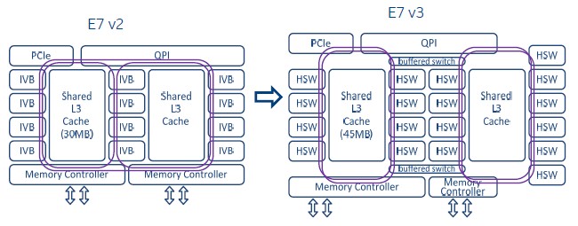
The Brickland platform is the combination of Xeon E7 processors, and the chart above shows how a four-socket configuration glues together using Intel’s chipsets. The Haswell Xeon E7 chips bring the voltage regulators onto the chip, which allows for more sophisticated power control and also lowers the overall power consumption of the next platform even as it does boost the thermals on the socket a bit.

The Brickland platform also includes Intel’s “Jordan Creek” scalable memory buffer chip, which is located on memory cards and which talks back to the memory controllers in the processing complex. This memory chip and controller combination now supports DDR4 main memory, which clocks a little higher and yet burns a bit less power compared to DDR3 memory. The memory controllers support the same three DIMMs per channel, and so a single socket supports up to 24 memory sticks and up to 1.5 TB of memory capacity using 64 GB memory modules and up to 3 TB of capacity using 128 GB sticks. (The use of 16 GB and 32 GB memory sticks is far more common on this class of machines because they cost a lot less per gigabyte.) This is the same memory capacity as was supported on the Ivy Bridge-EX Xeon E7 v2 processors from last year. If customers were expecting a memory capacity boost with the Haswell-EX processors, they are not going to get it, but the memory does run faster if customers want to move to DDR4.
Big Iron Is Big Again Thanks To In-Memory
In a world where large workloads are increasingly spread across clusters of relatively modest servers, the big iron machine might seem to be something of an anachronism. But shared memory machines that couple more than two sockets together to create a bigger logical machine for applications to run on still have their place – and some might even go so far as to say there could be a resurgence in big iron driven by in-memory transaction processing and analytics.
While such big iron machines, which last four or more processors together, are more expensive, they are in many respects a lot easier to program and are particularly well suited for applications that need to hold entire datasets in main memory. Such shared memory machines present a single logical processor to an operating system, which sees cores and threads as all part of a single virtual chip even though it may be as many as 16 or 32 chips in the box, with a dozen or more cores and anywhere from two to eight threads per core. (Some machines, like SGI’s UV 2000 and Oracle’s Sparc M series, scale even further than this.)
Some workloads – such as in-memory databases for transaction processing and queries and graph analytics to discover the relationships between members of a dataset – run best in the memory of a single system rather than a cluster. Scaling out the workload across multiple servers means leaving the memory subsystem to stitch together the dataset across an interconnect such as InfiniBand or Ethernet, and this incurs huge latencies between nodes that adversely affects the performance of the applications. This performance penalty is fine for certain kinds of parallel queries, where data is partitioned across the cluster, but it is not acceptable for most kinds of in-memory processing. It is a pity that symmetric multiprocessing (SMP) and non-uniform memory access (NUMA) system clustering technologies do not scale well beyond 32 sockets and do so cheaply. Some day, when the interconnects are fast enough and directly link all processing elements in a collection of server motherboards, there could be no practical difference between a cluster and a NUMA or SMP machine. (This is a dream, but not an absurd one.) In the meantime, customers have to carefully consider their applications before they choose a loosely coupled cluster or a shared memory machine.
And customers who want only a four-socket machine have to probably wait until Intel rolls out its Xeon E5-4600 v3 processors for four-way systems, probably in the not too distant future. The Xeon E7 v3 machines support much more memory and memory bandwidth as well as tighter coupling of the processors through Intel’s QuickPath Interconnect (QPI), which can mean significantly better performance for memory-heavy applications. But the Xeon E5-4600 v3 processors will be less expensive and come in much denser packaging from system makers, so there is that to consider, too.
The Haswell Tock
The Haswell generation of Xeons represents what Intel calls a tock in its tick-tock method of upgrading its server processors. Intel being a manufacturer, the shift to a new process technology for chip etching predominates, and in this case the tick was the move to 22 nanometer processes used across the Ivy Bridge generation of Xeons, including Xeon E3s for single socket-machines, Xeon E5s for two-socket and four-socket machines, and Xeon E7s for four-socket and larger machines. With a tock like the Haswell generation, Intel introduces a new microarchitecture in its cores, which cranks up the amount of work a core can do while using the same – and much perfected – manufacturing process used in the tick.
The next step to Broadwell is a tick, moving the slightly tweaked Haswell microarchitecture to the 14 nanometer process that has just been rolled out on the first Xeon, the Xeon D chip for microservers that Intel launched in March. Broadwell Xeon E5 processors are expected later this year, perhaps in September. And sometime in the next twelve to sixteen months, Intel will roll the 14 nanometer process up to the Broadwell-EX, probably about the same time as the next tock with the “Skylake” family of Xeons starts with 10 nanometer processes at the low-end Xeon E3 portion of the lineup.
With the launch of the “Haswell-EX” Xeon E7 v3 processors, Intel is turning the heat up a little more on its competitors, who are making their cases for their Power and Sparc motors and the systems that use them.
The top-bin Xeon E7 v3 processors have 20 percent more cores and 20 percent more L3 cache than their Xeon E7 v3 predecessors, which is not exactly a huge jump, but it is enough to make it worthwhile for both server buyers and server sellers. Because the clock speeds are a bit slower with the Xeon E7 v3 chips, the performance jump is a little bit less than 20 percent for many workloads, but it really comes down to cases. For certain workloads – particularly those that use floating point math – the performance improvement is considerably larger. It comes down to cases, as always. And The Next Platform has put together some basic performance data to help you consider the options, but doing your own benchmarks on your own code is the recommended course of action before making any big purchase.
To expand the core count on the Haswell-EX processors, Intel used the same strategy as it employed with the “Haswell-EP” chips for two-socket servers last September. The earlier Ivy Bridge processors had a set of three high-speed interconnect rings that linked the cores and their L3 cache segments to each other as well as linking to the two memory controllers, the PCI-Express controller, and the QPI links on the die. With the Haswell chips, Intel needed to get more cores on the die and so it created two sets of interconnect loops and linked them together by a pair of buffered switches. The two pairs of rings on the Haswell designs have the PCI-Express, memory controllers, and QPI links hanging off them, and any core can reach through the rings and switches and see any controller or cache segment. Here is what it looks like:
Conceptually, the Xeon E7 chips are what amounts to a baby SMP server in their own right, if you think of a core as a processor and a cache segment as main memory. Strictly speaking, this is not precisely true. But it is an example of how system functions are being pushed down to chips, if you take a very wide and long view of system design. SoC is not just happening on processors for our smartphones and tablets.
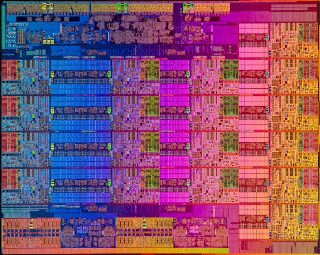
The Xeon E7 v3 processor has 5.7 billion transistors and has a die area of 662 square millimeters. Here is a more detailed block diagram that shows the innards of the Haswell-EX Xeon E7 v3 chip:
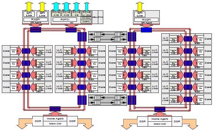
As you can see, Intel now has four columns of cores on the die, just like with the Xeon E5-2600 v3 processors for two-socket machines. And interestingly enough, the top-end Xeon E5-2600 v3 chip, the core counts were the same as for the Xeon E7 v3 chips (which come with a 4800 or 8800 designation, depending on whether they are enabled for four-socket or eight-socket machines). The L3 caches are the same size on these two processors as well, at 2.5 MB per core. The big difference between the Haswell E5 and the Haswell E7, aside from the differences in the sockets that they plug into and a bunch of RAS and other features, is that the Haswell E7 chip has three QPI ports rather than the two of the Haswell E5. The Xeon E7 variants also support twice as many memory slots per socket and therefore twice the main memory capacity as the Xeon E5 versions of Haswell. (The same held true with the Ivy Bridge versions.) The Haswell E7 is available on one die, with all eighteen cores on it, but there are actually three different physical Haswell E5 dies: one that has from four to eight cores, another that has ten or twelve cores, and the biggest one with from fourteen to eighteen cores.
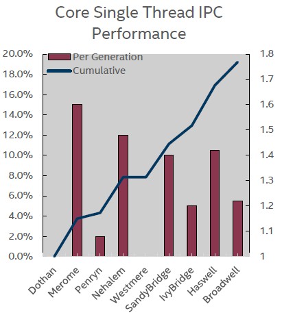
The important thing for big iron customers is that the new Xeon E7 v3 chips sport the Haswell cores. In a briefing at Intel’s facilities in in Beaverton, Oregon, Chris Gianos, the chip engineer who has steered the development of the Haswell Xeon E5-2600 v3, the Broadwell Xeon D-1500, and the Haswell Xeon E7 v3, walked The Next Platform through the architectural improvements that come through the Haswell cores. The first and most important one is that changes in the microarchitecture continue to push the amount of work a core can do per clock cycle. The instructions per cycle, or IPC, has gone up steadily over the years. (Intel reckons IPC improvements against the “Dothan” Pentium M cores from 2004.) The ticks (process change) always have lower IPC gains than the tocks (microarchitecture change), and this stands to reason. The jump from Ivy Bridge to Haswell is a biggie, and the jump next year to Broadwell for the Xeon E7 v4 chips will be more modest in terms of IPC, if the Xeon Broadwell D chip is any guide. Haswell gave a 10.5 percent kick to IPC, while Broadwell will only do about 5.5 percent, a tiny bit more than the Ivy Bridge improvement.
The Haswell cores have better branch prediction, deeper buffers, more table lookaside buffers, and more execution units, which all help push up the IPC versus the Ivy Bridge cores. The Haswell cores also have twice as much L1 and L2 cache bandwidth on their cores, and importantly sport 256-bit floating point and integer math in the AVX2 units and have dual fixed multiply add (FMA) units that provided twice as much performance in floating point math calculations compared to the Sandy Bridge and Ivy Bridge cores. (Specifically, the Haswell cores can do sixteen double precision floating point operations per clock per core, compared to the eight with the AVX1 units in the Ivy Bridge cores.) The AVX2 units in the Haswell cores also support 256-bit integer math operations with the Haswell cores.
Among the many other tweaks in the Haswell-EX E7s, the latest chips have QPI links that have a top speed of 9.6 GT/sec (that’s gigatransfers per second), up from 8 GT/sec with the Ivy Bridge E7 QPI links. This extra speed makes it possible the scale up the core count and the aggregate performance of the resulting machines.
The other interesting bit is that the Haswell-EX Xeon E7 processors support Intel’s Transactional Synchronization Extensions (TSX), which debuted with the Haswell cores. Because of a bug, this feature was disabled in the Haswell-EP Xeon E5 chips, but that “little bug,” as Gianos calls it, has been fixed and is now available in the Haswell Xeon E7 processors. And frankly, TSX is probably more suited to big iron customers anyway.

As The Next Platform has explained before, TSX removes the locking mechanisms that keep threads from manipulating the same data in main memory and lets all threads complete all of their work in parallel. In a normal system, when data is used by a thread, it is locked so no other thread can touch it, and that means other threads can stall even if they are only reading the data. By eliminating the locks at the front end and doing checks only after threads are done with their work, applications can run a lot faster. For instance, on HPC workloads, tests show TSX delivering about a 40 percent boost in performance on clusters, and Intel has also done performance tests on SAP’s HANA in-memory database using TSX, showing about a 2X boost from TSX alone. Moving from fifteen-core Ivy Bridge E7s running SAP HANA SP8 to eighteen-core Haswell E7s running HANA SP9 and turning on TSX boosted performance by 5.9X, according to Frank Jensen, performance marketing manager at Intel. The Sybase database is showing a 1.2X boost, and MySQL is being developed now to take advantage of TSX, according to Jensen. Oracle and DB2 databases will no doubt follow, as will PostgreSQL.
Another new RAS feature with the Xeon E7 v3 chips that enterprises will find useful that is new with the Xeon E7 v3 processors is called address range memory mirroring. “Several prior generations of the Xeon E7 chips had memory mirroring, but it was not the most popular feature,” explains Gianos. “The feedback was that memory is too expensive for complete mirroring.” And so Intel has tweaked the memory mirroring in the chip so it can be set for just a critical portion of memory and regulated by the operating system or the system firmware. Other RAS features include multiple rank sparing, which provides dynamic failover of up to four ranks of memory on each DDR3 or DDR4 memory channel, and that means a failed memory stick doesn’t take a machine down.
The Feeds And Speeds
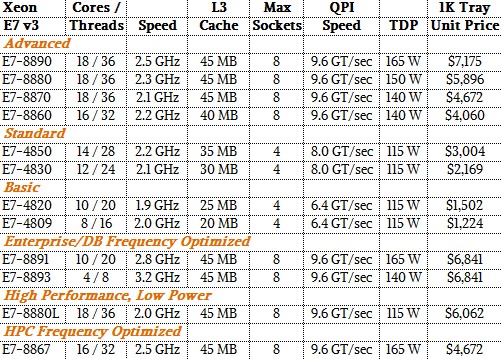
To make your life easier, we have put together a set of tables that detail the last three generations of the Xeon E7 processors – the Westmere-EX, Ivy Bridge-EX, and Haswell-EX chips. (Remember, Intel skipped Sandy Bridge-EX to close the gap between the entry and high-end rollouts of its server chips, and also because server makers did not want to engineer a Sandy Bridge-EX machine for what would have turned out to be a relatively short life.) Without further ado, here are the new Haswell Xeon E7 v3 chips:
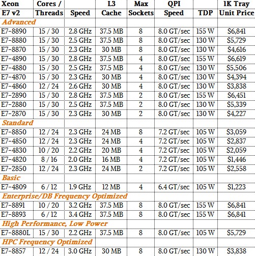
Here are the basic Ivy Bridge Xeon E7 v2 speeds:
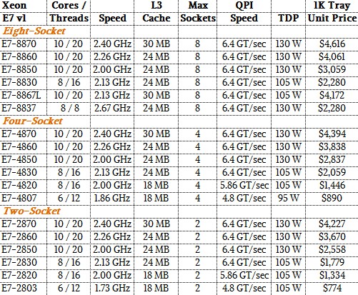
And going way back a few years, here are the details on the Westmere Xeon E7 v1:
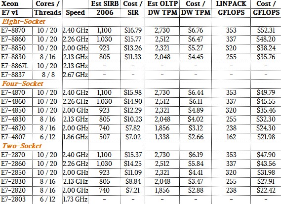
These feeds and speeds give you some sense of how the different chips line up within their generations and across the generations. To help even more with comparisons, The Next Platform has gathered up some performance statistics for these chips using a mix of integer, database, and floating point benchmark test results performed by Intel. With this data, you can start making rudimentary comparisons for performance and value across the Xeon E7 chips. Here is the performance table for the Haswell Xeon E7 v3 chips:
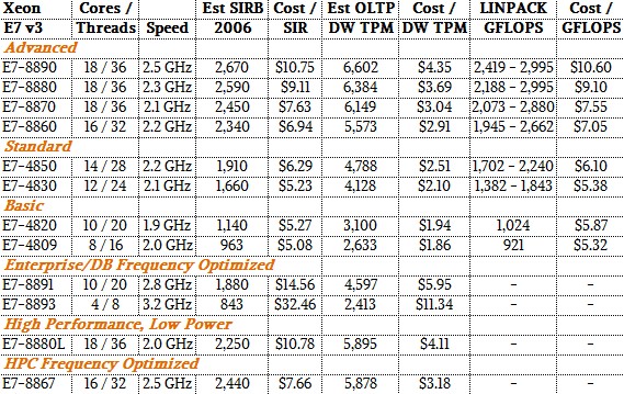
This table shows the performance of a single node with four of each processor type on three different tests. The first (Est SIRB) is the estimated integer processing performance as gauged by the SPECint_rate_2006 test. These are estimates provided by Intel and are in no way meant to convey that actual SPEC tests were done on all of the SKUs in the table. The second test, Est OLTP DW, is based on a benchmark that simulates a wholesale company managing the movement of inventory from its warehouses to its stores and that uses Oracle 11g as its back-end database. And finally, for floating point performance, which has seen a big jump thanks to the Haswell cores and their AVX2 units, Intel is using the LINPACK Fortran matrix math benchmark test.
There is one important caveat to the LINPACK results. First, with the AVX2 can consume a lot of juice when they are running heavily, and so Intel has broken the power controls for the AVX2 units from the execution units in the cores with the Haswell generation. This allows the cores to run at a slightly higher clock speed when AVX is not being used, and they have to gear down a bit when AVX2 is being used to stay in the thermal envelope of each chip. Because of this and other factors that come from variations in machinery, Intel is now providing a range of performance estimates for LINPACK instead of one figure. Our price/performance analysis in these tables takes the midpoint of the LINPACK range and shows the gigaflops that is delivered by a four-socket node. (The thing that jumped out immediately to us is that a single “Knights Landing” parallel processor coming sometime in the second half of this year will deliver a little more LINPACK performance than four eighteen-core Xeon E7 v3 chips. And probably with half the power consumption, too.)
Just for comparison’s sake, here are the performance stats for the Ivy Bridge Xeon E7 v2 chips:

And rounding out the set are the performance figures on the three tests for the Westmere Xeon E7 v1 processors:
Speaking very generally, the Xeon E7 v3 chips offer about 40 percent better performance on the top-bin parts than the Xeon E7 v2 processors they replace. If you do the comparisons for SKUs with the same names, the average improvement in bang for the buck comes to between 13 percent and 19 percent on the integer test, with some outliers offering more (like the Xeon E7-4809 v3 at 36 percent) and others offering less (like the top-end Xeon E7-8890 v3 offering 8 percent better oomph per dollar. For floating point work, the improvement in value is more like 2X because of the nearly doubling of LINPACK performance and the slightly lower cost per unit of performance. On database performance, the Xeon E7 v3 chips are showing something more like 25 percent to 45 percent improvement in price/performance, and this also stands to reason thanks to the addition of the TSX feature with the Haswell cores and the much higher cache memory bandwidth that is available, too. Add in the fact that customers will be able to get more memory capacity for the same dollar in their Haswell Xeon E7 systems, and databases should really scream.
Next up, we will examine the competitive landscape for the Xeon E7 v3 chips and who the likely customers will be for them.


The article states:
“for their Power and Sparc motors”
however, per Babbage, a difference machine or processor, today a CPU is an engine not a motor.
Park McGraw