
Given the exorbitant demand for compute and networking for running Ai workloads and the dominance of Taiwan Semiconductor Manufacturing Co in making the compute engine chips and providing the complex packaging for them, you would think that the world’s largest foundry would be making money hands over fist in the second quarter.
But alas, even with a hyperbooming AI system sales, that market is still small enough – and the amount of money that TSMC gets from etching and packaging chips is small compared to their street prices – that when the smartphone, PC, and generic server markets all take a bit of a dive at the same time, sales of AI compute engines are not enough to fill in the gap.
Like this, in fact:
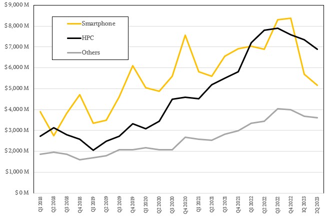
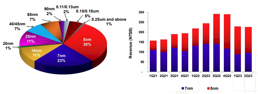
Remember: When TSMC says “HPC” it means the etching of high performance chips used in PCs, servers, storage, and switches, it does not mean HPC simulation and modeling only. AI chippery is in that black line above, and you know it is because the black line has been growing like crazy in recent years and has not fallen off a cliff compared to smartphones, which are clearly struggling in the past two quarters. For the past five years, smartphones drove about half of TSMC’s revenues, but in the past two quarters the HPC segment (as defined above) has become dominant and is expected to be so for the foreseeable future.
On a conference call with Wall Street analysts, CC Wei, vice chairman and chief executive officer of the foundry, said that the manufacturing of GPU, CPU, and custom ASIC compute engines for AI inference and training represented only 6 percent of its total revenues, which came to $15.68 billion and which means AI products only drove $941 million in revenues. You can probably attribute some InfiniBand and Ethernet ASIC manufacturing to AI on top of this number, but you get the idea. Companies like Nvidia are making a whole lot more coin on AI than TSMC is, and that shows you that while manufacturing and packaging are important, design and sales drives a lot more revenues and, presumably, a lot more profits.
Translation: It is good to be ASML, it is great to be TSMC, but it is absolutely fabulous to be Nvidia.
“The recent increase in AI-related demand is directionally positive for TSMC,” Wei said on the call with Wall Street analysts. “Generative AI requires higher computing power and interconnect bandwidth, which drive increasing semiconductor content. Whether using CPUs, GPUs, AI accelerators, and related ASICs for AI and machine learning, the commonality is that it requires use of leading edge technology and a strong foundry design ecosystem. These are all TSMC’s strengths.”
Looking ahead, Wei said that TSMC expected for AI in its many guises to drive somewhere in the “low teens” of its revenues in the next five years, with a compound annual growth rate of close to 50 percent. Depending on where you think TSMC’s revenues will be in five years, AI will drive maybe $3.7 billion in revenues in 2023 (assuming a pretty good second half for AI and a slightly growing growth rate), and a CAGR of 48.5 percent (which we picked arbitrarily) puts it at around $18 billion. If that represents “low teens” of overall revenue – call it 13 percent for fun – then TSMC will be somewhere above $135 billion in overall revenues in 2027 by this model.
TSMC is therefore projecting to more than double in revenues between now and 2027, and AI revenues will go up by nearly 5X. But AI is not the only, or the biggest, driver of revenue growth. The desire to put more chips in more things with more advanced processes to deliver the best performance per watt – with PCs, smartphones, tablets, IoT devices, car chips and systems, and myriad edge and embedded devices – is what is driving this growth, and AI is but one example of this.
Isn’t math fun?
In the quarter ended in June, net income at TSMC fell by 26.5 percent to $5.93 billion against that $15.68 billion in sales, which was off 13.7 percent. The PC and smartphone industry burndown is taking longer than expected, and the recovery of the economy in China that TSMC and others were banking on has not materialized. And so the drop in sales. Costs for the development and ramping of 3 nanometer and 2 nanometer processes, the former which is ramping now for shipments later this year, are rising, which is also putting pressure on profits. And the ongoing investment in capital equipment, including a very expensive factory that TSMC is building in Arizona, has forced TSMC to burn down $4.38 billion of its cash hoard to run the company and to make $8.17 billion in capital expenses for new foundries and equipment. That said, capital spending was up 10.4 percent compared to the year ago period, and the company is still on track to spend about $34 billion on capital expenses this year, which is still an extraordinary amount of money.
As Wei is fond of reminding everyone, TSMC has to spend many years in advance of a technology trend that it hopes will materialize. As it grows along with semiconductor demand, the bets keep getting bigger, but not in relation to the semiconductor total addressable market. What TSMC is doing is exceedingly hard, and it is really the only one that is delivering advanced processes and packaging in the volumes and at the technology nodes in volume. Intel has a long way to catch up, and Samsung is very particular about what compute it runs through its fabs, which are mostly geared for memory. These are pretty much the only options available right now, unless you are a Chinese company, in which case you have to rely increasingly on Semiconductor Manufacturing International Corp, the indigenous foundry that cannot get its hand on extreme ultraviolet light (EUV) technologies that are required to move to 5 nanometers and below.
At the moment, TSMC is being cautious about how the second half of 2023 will look, given that it missed how long the inventory burndown and the recovery in China would take, but says that it expects for sales to be down around 10 percent this year, which would put it at $68.3 billion for the year. Given the costs of the building foundries in the United States, Japan, and Europe and the 3 nanometer ramp, profits will very likely be under similar pressure and TSMC could see the kind of declines in net earning (around 2X the rate of revenue declines) that it saw in Q2.
No matter how much pressure TSMC is under, it is nothing like the Jupiterian gravity that Intel is under. And it is still making money and it still has $47.86 billion in cash at the moment.
What TSMC does not have are foundries that are cranking out chips at full speed, which is how a foundry makes profits – it is the only way that any foundry makes profits. One of the reasons why sales in its HPC sector are not higher is that they are gated by the back-end Chip on Wafer on Substrate (CoWoS) silicon interposer technology that a lot of compute engine makers are using to create their devices; some are using chiplets, others are using monolithic chips or chiplets in combination with HBM stacked DRAM memory. Wei was vague, but said that TSMC is at least doubling its CoWoS capacity this year, but reminded everyone that this takes time.
The chip foundry itself is not a bottleneck, but the packaging is. AMD was limited by the availability of substrates for the past two years for its Epyc server CPUs, and CoWoS is a limiter for GPUs and FPGAs. Going forward, all chip makers are going to have to be very careful that they line up both wafer etching and packaging.
What is immediately obvious is that TSMC has plenty of capacity to crank out 7 nanometer chips and a bunch of capacity for 5 nanometer chips. And these will be long-lived nodes, just like the 3 nanometer processes that are currently ramping will be. We don’t think companies making mainstream CPUs and GPUs are stalling their 5 nanometer projects to intersect with 3 nanometer processes, but given the state of the global economy, maybe they are stretching a bit to heavily invest in 3 nanometer technologies. More than a few AI ASIC makers are sitting on generations of machines that are a few years old and they are not talking about compute engine upgrades, for instance.
It is significant that with the jump from 3 nanometers to 2 nanometers, there is not as big a performance or density jump as from 7 nanometers to 5 nanometers. But it is important that there is a much bigger increase in power efficiency, which everyone is looking for in devices large and small.
Wei gave an update on its 3 nanometer and 2 nanometer ramps, as he has been doing for the past several quarters. The N3 and N3E processes, he bragged, will lead the industry in terms of power, performance, and area and underlying transistor architecture.
“N3 is already involved in production with good yield,” Wei said. “We are seeing robust demand for N3 and we expect a strong ramp of N3 in the second half of this year, supported by both HPC and smartphone applications. N3 is expected to continue to contribute a mid-single-digit percentage of our total wafer revenue in 2023. N3E further extends our N3 family with enhanced performance, power, and yield, and provides complete platform support for both HPC and smartphone applications. N3E has passed the qualification and achieved performance and yield targets and will start volume production in the fourth quarter of this year.”
Wei added that N2 development, using nanosheet transistors comparable to Intel’s 18A process, is on track for volume production in 2025, and will give a full node performance increase and power decrease as well as a new feature called backside power rail, which will provide a 10 percent to 12 percent increase in speed and a 10 percent to 15 percent boost above and beyond the node shrink for chips etched using the N2 process. The backside power rail feature will be available in the second half of 2025 and will be in customer production in 2026.
And despite what Intel is claiming about transistor supremacy in 2025 with its 18A process, Wei said N2 will be the best in either the West or the East.
What the industry needs is two foundries at around the 2 nanometer node, and hopefully they are neck and neck and yielding well.

Dell Gives A Second Opinion On Enterprise IT Spending
Like many of you, we are trying to find out what the heck is really going on in the global economy. And as such, we are paying particularly close attention to the original equipment manufacturers, or OEMs, who peddle servers, storage, and often switching into the enterprise. They are leading …
When Push Comes To Shove, Google Invests Heavily In GPU Compute
A year ago, at its Google I/O 2022 event, Google revealed to the world that it had eight pods of TPUv4 accelerators, with a combined 32,768 of its fourth generation, homegrown matrix math accelerators, running in a machine learning hub located in its Mayes County, Oklahoma datacenter. It had another …
Intel Delays “Sapphire Rapids” Server Chips, Confirms HBM Memory Option
It is a relatively quiet International Supercomputing conference on the hardware front, with no new processors or switch ASICs being announced from the usual suspects. While Trish Damkroger, general manager of Intel’s high performance computing division, gave the keynote opening up ISC 2021, providing a little more insight into the …
TSMC may be getting only a bite of the AI pie but the memory makers are surely getting a big bite as well given the. Manufacturing cost of the HBM in hopper is more than the cost of the H100 due itself by some way.
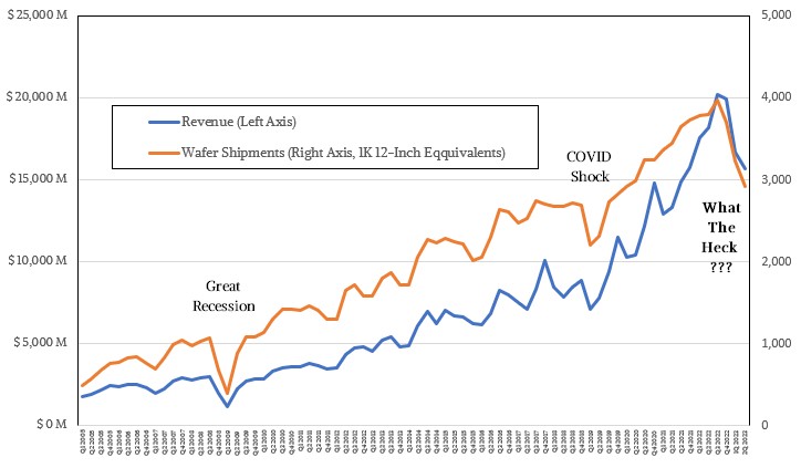
Phew … that “What the Heck???” drop in wafer shipments is rather roller-coaster puzzling indeed! It looks to me like recoil from the awesome climb that followed COVID Shock.
I foretell that the January ’24 report, for Q4, will have wafer shipments at 3,500 1K-12″-eqs, or better (and somewhere in-between for Q3 in October, maybe 3,200) — that’s what the long-departed spirits from my non-AI crystal ball incantations are seeing for that timeframe … 8^q
So who didn’t plan? AI chip guys or the foundry? That drop off in wafer shipments could have some improvement if not gated by CoWoS. The demand is obviously there. AMD, Nvidia, Intel, they’re all using this chip stacking and have been using for years now. So it looks like TSMC made their own bed here by not building out the capacity sooner. But yes, I’m sure they didn’t anticipate the huge impact of ChatGPT either.
Exactly.