
It was absolutely inevitable that China would try to create its own GPU compute engines. It was never a given that it would succeed in only three years.
But with the launch of the BR series of products from Biren Technology, there is finally a credible homegrown GPU controlled by China for graphics and compute, and that is going to add even more competition to the already intense GPU market.
Back in 2019, the trade war between the United States and China was escalating and the Middle Kingdom had long-since been prevented from buying compute engines for its HPC system aspirations. And so Zhang Wen, a serial entrepreneur who, among other things, worked to helped China make better LED chips at a startup created by Zhang Rujing, the founder of Semiconductor Manufacturing International Corp (SMIC), China’s largest chip foundry, decided that China needed its own GPU for computer graphics as well as for numerically intensive high performance computing.
A number of companies have tried, but Wen’s company, presumably named after the Hindi term for “lord of warriors” and not the old English for “at the barn,” has started shipping its BR104 and BR100 GPUs and showed them off at the Hot Chips 34 conference this week.
This is a pretty fast ramp for a GPU to come to market, obviously. Wen put together a chip design team with GPU experts from all over the world, and raised around $800 million through the beginning of this year to fund the research, development, and manufacturing of the chips, the latter of which is done not at SMIC, but across the South China Sea in Taiwan – specifically at Taiwan Semiconductor Manufacturing Co, the world’s most important foundry, and specifically using its mature 7 nanometer processes.
Assembling The Team
Biren was co-founded with Lingjie Xu, who was a senior GPU architect at Nvidia from 2008 through 2010, then a GPU architect at AMD for two years after that before taking a job as manager of GPU architecture at Samsung for five years after that. Significantly, Xu then became a director at Alibaba Cloud, the cloud division of the Chinese hyperscaler that is one of the Magnificent Seven top IT buyers in the world. (It’s a fair guess who is in the front of the line to buy Biren’s GPUs. . . .) Xu is head of products at Biren, and Wen is chief executive officer.
Wen and Xu hired two important people to get this job done. One was Mike Hong, who was vice president of architecture at GPU maker S3 (bought by Via Technology in 2013) from 2007 through 2016 and chief GPU architect at the HiSilicon chip development spinoff of Huawei Technologies. Wen hired Hong to be chief technology officer at Biren in January 2020. And a year ago, Wen tapped Allen Lee, who used to run AMD’s R&D center in Shanghai as well as running its business with China. With the successful launch of the BR104 and BR100 GPUs, it is no wonder that Biren has a market valuation approaching $3 billion, and there will probably be tremendous pressure for clouds, hyperscalers, enterprises, and IT manufacturers in China to buy its GPUs.
It was Hong and Xu who unveiled the Biren GPU architecture at Hot Chips.
One Tapeout, Many SKUs
Biren had two goals when it started its GPU design, according to Hong. The first was not just deliver a big GPU compute engine, but rather to make multiple GPU products from a single tape out. And that is why the Biren products are based on a chiplet architecture from the get-go. The second design spec for Biren was to deliver a GPU that had 10X the performance of the 2019-class of GPUs when it came onto the market, estimated back then as being sometime in 2022 according to Hong.
Biren has definitely delivered on the latter, which is amazing given the short runway. Figuring out if Biren hit the second target is a bit more complex.
“As we envisioned the model size of deep neural networks will continue to grow exponentially, the datacenter compute deficit will also be widened,” Xu explained in his Hot Chips session. “We saw that when the BR100 would come out in 2022, it should be roughly 10X the performance of the 2019 standard. This meant we had to raise the bar from hundreds of teraflops to 1 petaflops. That was why we set 1 petaflops mixed-precision 16-bit tensor flops performance as the target. And we did it.”
Nvidia was halfway between the “Volta” GV100 GPU from 2018 and the “Ampere” GA100 GPU at the time of Biren’s founding. If you look at INT8 performance of the BR100 compared to the Volta and Ampere GPUs from Nvidia, this seems roughly on that 10X target.
As for FP16 running atop matrix math units – what Nvidia calls FP16 Tensor Core – Volta was at 125 teraflops and Ampere was at 312 teraflops but at 624 teraflops with sparse data, which Nvidia knows how to double up through the GPU with math tricks. If you average that Volta and Ampere performance without sparsity, you get 218.5 teraflops; 10X that is 2,185 teraflops. Using the BF16 16-bit Bfloat format created by Google, the BR100 does a respectable 1,024 teraflops. Biren hit the target it set in 2019 for what it expected 2022 performance to be, but Nvidia moved the goalposts out – and they are even further out with the H100 GPU.
Here is how Biren says it stacks up on various machine learning workloads, pitting the BR100 against the Nvidia A100:
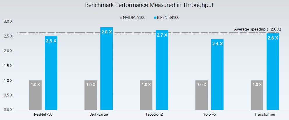
We presume this is for AI training workloads, not inference. The average speedup over the A100 is around 2.6X. It is not clear if the Nvidia machines were using sparse matrix features, which doubles the throughput, or not. Our guess is they were not.
The BR104 and BR100 GPU accelerators support all kinds of numerical formats, including INT8, INT16, and INT32 for integer data and FP16, BF16, a new format called TF32+ (a variant of the 32-bit Tensor Format floating point created by Nvidia for the Ampere GPUs), and regular FP32 single precision. There is no FP64 double-precision floating point, which limits the use of the BR series of GPUs for certain HPC simulation and modeling workloads that require 64-bit processing. (This can always be added later in a rev of the chip, and there are multiple ways to do this concurrent with a process shrink.)
In keeping with the naming conventions of Nvidia GPUs in recent years, the “100” model is the full beast aimed at heavy GPU compute, while the “104” model is a smaller device aimed at graphics and inference workloads as well as compute. With Nvidia, these classes of machines are done with GPUs with a different architecture, but with the first round of products from Biren, the low-end product is a single Biren GPU and the high-end product is two of these chips lashed together with a high-speed, chip-to-chip interconnect.
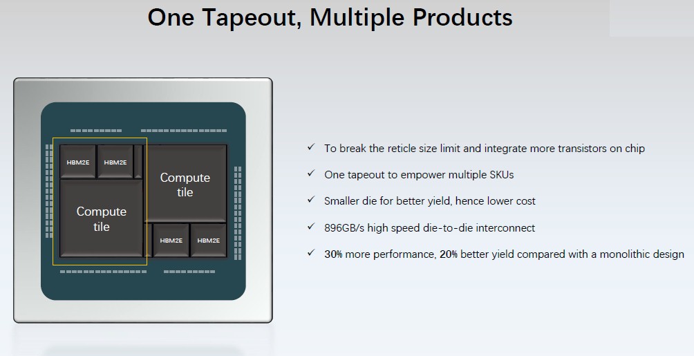
As is well known by now, smaller chip dies have better yields and therefore they also have lower cost. The way the two-chiplet Biren GPU complex works, the yield across two chiplets is 20 percent higher than would be possible on a monolithic design, and because it busts out of the reticle limit at TSMC’s fabs, Biren can deliver 30 percent more performance than it could have done with a monolithic design as well.
With the datacenter market pretty much all to itself for the past decade, Nvidia has not had to care about GPU costs the way it will going forward with a resurgence AMD, an eager Biren, and a damned hungry Intel pushing their GPUs against Nvidia’s monolithic designs. Nvidia will inevitably move to chiplets, and has laid the groundwork for this, as we talked about back in January.
Here is a shot of the high-end BR100 package with two of the GPUs inside along with its basic feeds and speeds:
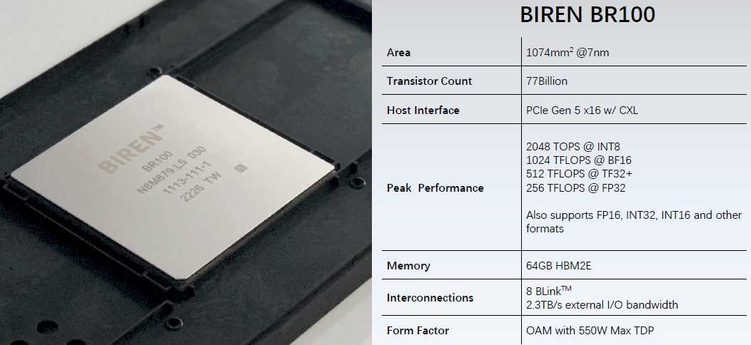
The BR104 chip has 38.5 billion transistors and therefore the BR100 dual-chip module (DCM) has 77 billion transistors. That is more than the 54 billion transistors that Nvidia had with the “Ampere” A100 GPU accelerator and just shy of the 80 billion transistors that Nvidia was able to squeeze into the Hopper H100 GPU accelerator and squeeze out of TSMC’s 4N process. This 4N process is a refinement – and what we presume is an expensive refinement – of TSMC 5 nanometer process that Biren will probably use on its next generation product.
Biren designed the BR100 series to plug into PCI-Express 5.0 x16 slots, and like every other GPU maker finds itself waiting for Intel to deliver its “Sapphire Rapids” Xeon SP CPUs and for AMD to deliver its “Genoa” Epyc CPUs, which may be branded as the Epyc 9000s if the rumors are right. (We have been calling them the Epyc 7004s to be consistent with the naming convention with the prior three generations of AMD CPUs.) IBM is delivering PCI-Express 5.0 slots with its “Cirrus” Power10 processors, just launched in entry and midrange machines back in July, but Biren will very likely not support the Power Systems machines or their Inspur clones. Ampere Computing, which has had some success selling its Altra and Altra Max Arm-based servers to Chinese hyperscalers and cloud builders Alibaba, Baidu, and Tencent, is not expected to support PCI-Express 5.0 until next year’s AmpereOne-2 chip, which we have dubbed “Polaris” in the absence of a codename from the company.
The BR100 chip supports four stacks of HBM2e memory with a total of 64 GB of capacity and 1.64 TB/sec of aggregate bandwidth.
The GPU accelerator links to host machines over the PCI-Express 5.0 bus but also includes an eight-way, all-to-all interconnect called BLink that is akin to a kind of NUMA interface for the GPUs. This BLink interconnect is the heart of the server design for Biren’s GPU accelerated system, which is understandably called the Hearten Server. It is unclear what the BLink protocol is, but we strongly suspect it is a cache coherent protocol that uses PCI-Express 5.0 as a transport but runs a leaner and meaner protocol, maybe even CXL or OpenCAPI, maybe a homegrown NUMA protocol.
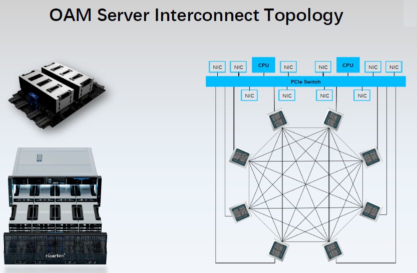
The interconnected BR100 GPUs fully share that HBM2e memory over a 2.3 TB/sec all-to-all network, and they all link to each other and to host CPUs and to network interface cards thought a slower PCI-Express fabric.
The BR104 will be packaged up in PCI-Express card form factors, while the BR100 comes in an Open Compute Accelerator Module (OAM) form factor that was co-developed by Microsoft and Facebook in 2019, the year Biren was founded, and that is being increasingly adopted by accelerator makers.
Breaking Down The BR100 Architecture
The Biren GPUs are organized in a similar fashion to other GPU compute engines, which is no surprise given where Biren’s engineers come from and how compute needs to be organized to scale massively across threads and hide latencies with caches.
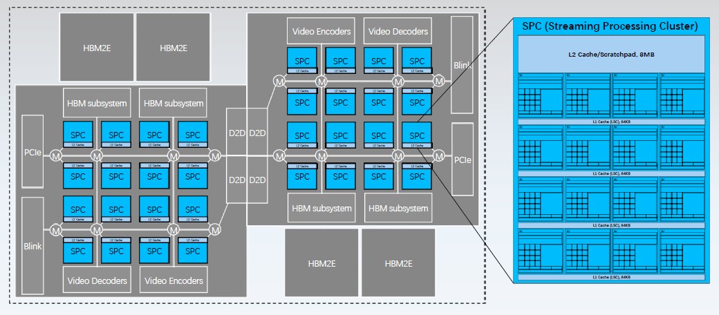
Each B104 chip has sixteen streaming processors, which Biren calls streaming processing clusters, or SPCs for short. These SPCs share an 8 MB distributed L2 cache and scratchpad memory and are interlinked to each other and to various controllers over a high speed mesh on the die.
The two BR104 chips are connected through a pair of die-to-die interconnects. At 896 GB/sec, that D2D interconnect offers essentially the same bandwidth as the 900 GB/sec NVLink 4 ports that are lashing together the future “Grace” CPUs from Nvidia to each other and to the impending “Hopper” H100 GPUs in a superchip complex. The fact that this D2D interconnect has so much bandwidth means that the BR100 looks like a single GPU to software; this is not the case with the “Aldebaran” Instinct MI200 series of GPUs from AMD, which are co-packaged and interconnected, but which look like two GPUs to the ROCm software stack.
Each BR104 die has a PCI-Express 5.0 controller and a BLink interconnect controller. There are two sets of video encoders that make these BR104 chips real GPUs, not just compute engines.
The BR104 SCM burns 300 watts, while the BR100 DCM burns 550 watts, which suggests that the DCM version is clocked down a bit to stay within the same thermal envelope as Nvidia, AMD, and Intel are targeting.
Let’s drill down into the SPC’s execution units, or EUs:
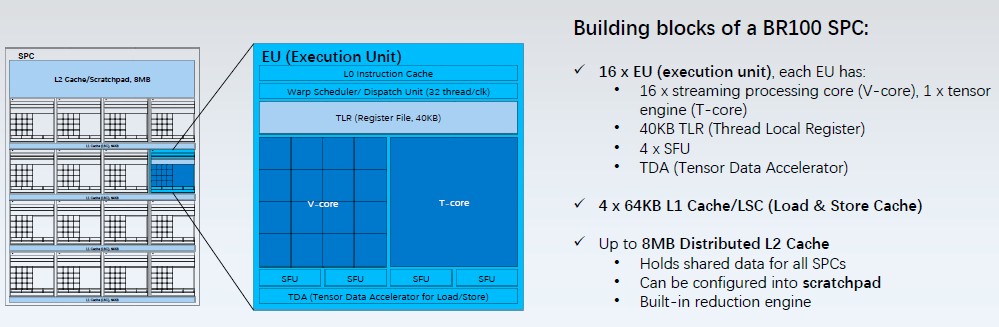
Each EU has 16 vector cores (V-cores) and one matrix math tensor core (a T-core). The V-core uses an enhanced SIMT model, according to Hong, which allows for 128,000 threads to run across 32 SPCs. (Each EU can schedule 32 threads per clock on its warp scheduler/dispatch unit.) V-cores do INT16, INT32, FP16, and FP32 processing. The T-core does the 8×8 matrix multiplication and addition (MMA) processing commonly used in the convolution layers of a neural network. This unit supports the TF32+ format created by Biren as well as INT4, INT8, INTE16, BF16, and FP32 processing. And interestingly, all of the T-cores on an SPC can be aligned to do the equivalent of a 64×64 MMA operation.
The TF32+ format has an 8-bit exponent and a 15-bit mantissa, which has five more bits of mantissa than normal TF32 and therefore 32X more precision, but is still not as dense numerically as full-on FP32, which has 8 bits of exponent and 23 bits of mantissa. If looks like this TF32 support is based on double-pumping the BF16 multiplier.
There is a tensor data accelerator that speeds up the load/store operations for both types of cores by offloading memory address calculation from the load/store units. It also supports different tensor layouts (from 1D to 5D). The EU has four special function units (SFUs), which execute special functions just like the SFUs in the Nvidia architecture does. The V-cores and T-core share these as well as a 40 KB thread local register (TLR). The EU is fronted by a Level 0 instruction cache (size unknown) The SPC has four 64 KB L1 caches, which for some reason are not shown in the diagrams.
One neat bit about the Biren GPU architecture is that EUs can be dynamically allocated to a higher level construct called a compute unit, or CU, which can have 4, 8, or 16 of the EUs in them, synchronized across their threads as if they were a kind of virtual streaming processor.
As for software, Biren had to come up with its own stack, which is called BirenSUPA:
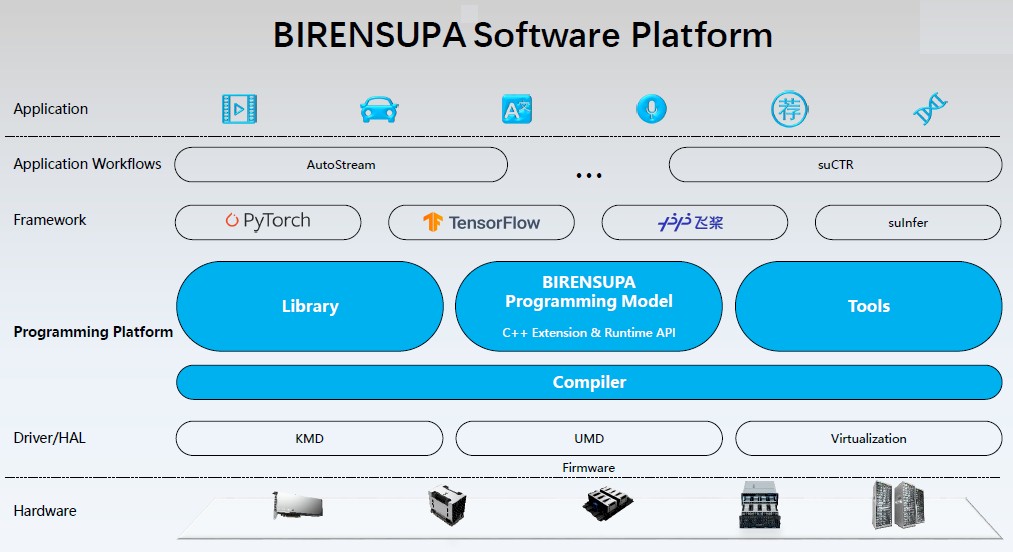
This software stack is conceptually similar to Nvidia’s CUDA, but it is not compatible.

Balancing AMD’s Future On The Edge Of A Silicon Wafer
The hardest job at any chip designer that doesn’t actually own its own foundry – and maybe even those that do – is figuring out what wafer start commitment level to make for a new compute engine in the datacenter. Guess too low, and you are supply constrained. Guess too …
What To Do When You Can’t Get Nvidia H100 GPUs
In a world where allocations of “Hopper” H100 GPUs coming out of Nvidia’s factories are going out well into 2024, and the allocations for the impending “Antares” MI300X and MI300A GPUs are probably long since spoken for, anyone trying to build a GPU cluster to power a large language model …
With ROCm Software And Instinct MI200 GPUs, AMD Has Ecosystem Critical Mass
Paid Feature Great hardware is the foundation of any compute platform. But hardware, in and of itself, is never sufficient to create a platform. And in fact, it takes two other important things for any platform to be realized. After the hardware, a platform requires a complete stack of software …
At least Intel can feel superior to somebody…
Can it play crysis??
I believe with the right AI software, IT can play Crysis! HA!
Thanks for the informative article. Just a small correction on the origin of the name “Biren”; it’s actually based on the first and last characters from a Chinese four-character idiom 壁立萬仞 (bì lì wàn rèn), which can either mean steadfast determination or insurmountable heights.
Sources:
https://www.birentech.com/news/112.html Biren themselves on the origin of their name (second pic, read the red characters right to left)
https://www.zdic.net/hans/%E5%A3%81%E7%AB%8B%E8%90%AC%E4%BB%9E Definition 1 of bì lì wàn rèn
https://kmcha.com/cidian/%E5%A3%81%E7%AB%8B%E8%90%AC%E4%BB%9E Definition 2 of bì lì wàn rèn