

There has been talk and cajoling and rumor for years that GPU juggernaut Nvidia would jump into the Arm server CPU chip arena once again and actually deliver a product that has unique differentiation and a compelling value proposition, particularly for hybrid CPU-GPU compute complexes. And today, at the GTC 2021 virtual conference, Nvidia co-founder and chief executive officer Jensen Huang is going to announce just that by unveiling its “Grace” Arm server CPU effort.
No, you didn’t have too much of the brown acid and you are not having flashbacks, although you can be forgiven for wondering if you did, considering how Nvidia laid out a plan in January 2011, called “Project Denver,” to add Arm cores to its GPU accelerators (much as the FPGA makers Intel/Altera and Xilinx were doing then and still do now) to displace inefficient X86 processors in the datacenter. Unlike those FPGA accelerators, which have a modest amount of compute, the Denver hybrid processors were supposed to have both beefy CPU and beefy GPU capacity and obviate the need for an X86 processor entirely.
It was the right idea, we thought at the time, and we think it is the right idea today, too, even as Nvidia is pursuing its $40 billion acquisition of Arm Holdings, the company that owns the intellectual property behind the Arm architecture, which is licensed to hundreds of chip designers who ship 20 billion devices a year.
The world is a lot different today than it was a decade ago. Back in January 2011, the Armv7 architecture was stuck at 32-bit processing with an expected 40-bit memory addressing expansion in the works, and the Armv8 architecture with its 64-bit processing and memory addressing – which X86 and other RISC processors had at the time – was still unannounced and years into the future in production chips. The Arm ecosystem was slow to mature in the server space, and Nvidia can be forgiven for quietly pulling the plug on Project Denver server SKUs, although we did catch wind of the Tegra K1 “super chip” with two Denver cores plus 192 CUDA cores way back in 2014. When IBM added NVLink ports to Power8+ and Power9 and Nvidia went after the supercomputer market with Big Blue as a team, Denver server CPUs became redundant. But all that work on the custom core – including the emulation of the Arm ISA top of a proprietary Nvidia ISA with a translation layer in-between like Transmeta was trying to do all those years back (and which might allow Denver cores to emulate X86 instructions but no one ever said that out loud) – was never used as far as we know. But it may be given new life.
Everything that Nvidia and the market has learned about CPUs in the past decade can be brought to bear in Grace CPUs, and now Nvidia itself is big enough to be the primary contractor for exascale-class machines or at the very least supply the CPU and GPU compute as well as the networking and DPU offload engines to a supplier such as Hewlett Packard Enterprise, which really doesn’t mind making custom variants of its “Shasta” EX supercomputers. And that is precisely what will be happening with the future “Alps” supercomputer going into the Swiss National Supercomputing Center in early 2023, featuring a hybrid compute module that has the homegrown Grace Arm server CPU very tightly couple with a future Nvidia GPU accelerator. This Alps machine will be the kicker to the current “Piz Daint” Cray XC30/XC40/XC50 system based on Intel Xeon E5 processors and Nvidia P100 GPU accelerators that was initially rolled out in 2013 and upgraded over the next several years to have a total of 5,704 nodes with a peak double precision floating point performance of 27.15 petaflops. The Alps machine will deliver 20 exaflops of performance, presumably at half-precision floating point, which if you were just using the FP64 cores on the GPU would mean it would be a 5 exaflops machine at double precision if the CPUs and GPUs both support FP64. We assume Alps is also making use of sparse matrix acceleration, which means it is akin to a 2.5 exaflops machine as we count them today, and also running this on the TensorCores, not the FP64 units, and that is more like a 445 petaflops machine at regular FP64 oomph. (Thanks for the catch on that, Matt.) Still, that’s nothing to sneeze at, even in the 2023 timeframe. What Nvidia has also said is that the Alps machine will be 7X faster than the “Selene” system that Nvidia has built for itself based on several generations of its own GPU accelerators, which is how you get to an FP64 estimate of 445 petaflops by working it backwards.
That future Nvidia GPU in the compute module for the Alps supercomputer was unnamed in the announcement at GTC 2021 today, but depending on the rumors could be either called “Hopper” or “Lovelace.” These code-names refer, of course, to Grace Hopper, who came up with the idea of machine-independent programming languages and wrote some of the first compilers on early computing systems, and Ada Lovelace, the mathematician who worked on programing the Analytical Engine built by Charles Babbage. It makes sense that the hybrid compute model would have the code names “Grace” and “Hopper” so we suspect this is the case. But, product roadmaps fold up in funny ways sometimes and vendors don’t always get to their precise destinations on time. So we shall see.
CSCS is not alone in getting a Grace-Hopper supercomputer. Los Alamos National Laboratory, one of the Department of Energy national labs in the United States, will also be getting a Grace-Hopper supercomputer from HPE in early 2023. This is not surprising, with Marvell pulling the plug on the “Triton” ThunderX3 server, leaving Los Alamos with no upgrade path for the “Thunder” cluster built by HPE and Marvell and the companion “Astra” Arm cluster at Sandia National Laboratories; both machines were installed in 2018. Given some of the features of the hybrid compute module and its interconnect, we think that Nvidia will have more than a few supercomputing centers and AI centers knocking on its door for these machines. We also think, of course, that Nvidia will build its own Grace-Hopper machine and it will be a top-ranked system in the HPL and HPL-AI benchmarks and do pretty well on the HPCG and Green500 and ML-Perf rankings, too.
Let’s take a look under the hood:
We spoke to Paresh Kharya, senior director of accelerated computing at Nvidia, about the Grace CPU and the hybrid CPU-GPU compute module and the architecture, in a very general sense, of the systems that will use it.
As you well know, we have said for quite some time – and said so to Huang ourselves last year when we were talking about datacenter infrastructure architecture after the GTC fall event – that what someone needs to do is create a superfast CPU that has all of its vectors ripped out because we know they are going to offload all the complex math to the GPU and then crank up the clocks and the cores has high as makes sense to make a screaming serial processor with big fat DRAM memory to counterbalance the parallel GPU motors with their screaming fast HBM2 memory. Slap a shared memory space across these, and off you go, you have a balanced hybrid architecture. This Grace Arm server CPU will not push it quite that far, and that is because Kharya cautions us that not all codes running on these exascale-class machines can run in hybrid CPU-GPU mode. Maybe someday, but that day is not today, or in 2023. (We are always talking about the next platform, and this one may be a technology of the future that is always in the future. . . . ) To be super-specific, there are elements of HPC simulation and modeling workloads and of AI training workloads that need to do math on the CPU and take advantage of the clock speed of that CPU and its large memory. You can’t ignore that, or you get an Amdahl’s law issue.
So, we can infer from this – since Kharya did not really talk about the core architecture of the Grace chip – that the Grace chip will have a mix of serial and parallel elements on it. The chip is also going to be build on a future Neoverse core, what Kharya called a “next generation, high performance core.” If we were Nvidia, we would not be using the “Zeus” V1 core or the “Perseus” N2 core, which were detailed by Arm Holdings back in September, even though the V1 has a pair of 256-bit SVE vector units and 50 percent more single-threaded performance than the current “Ares” N1 cores coming to market now in several processors, including the Graviton2 from AWS and the Altra from Ampere Computing. The N2 core is less impressive than the V1 in terms of performance, with only a 40 percent uplift in single-threaded performance and only a pair of 128-bit SVE vector units, but the N2 does have the virtue of supporting the new Armv9 architecture that we talked about a few weeks ago. We think it is far more likely that Nvidia will use a future “Poseidon” core, which is due to be released by Arm Holdings in 2022 or so, which will had a 30 percent uplift in single-threaded performance and vector performance boosts, too. (These may have a V2 and N3 variant; they may not.)
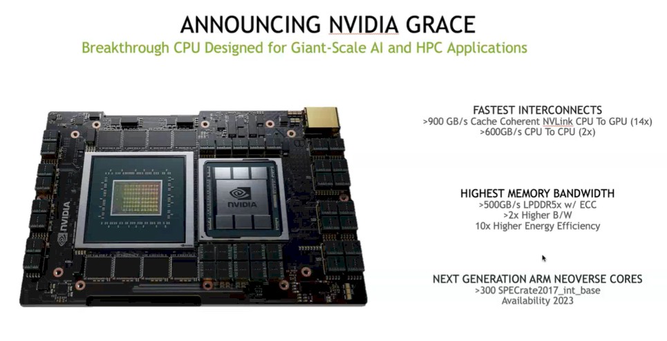
What we do know for sure is that Nvidia is committing to delivering an integer performance of over 300 on the SPECrate2017_int_base test, which is on par with a pair of 28-core “Skylake” and “Cascade Lake” Xeon SP processor from Intel.
The Grace CPU will support low power DDR5 with 500 GB/sec of bandwidth, and because it is using the low power variant of DDR5 aimed at laptops, it can deliver 2X the bandwidth of a normal two-socket X86 server and what Nvidia claims will be a 10X better thermal efficiency per bit moved.
The future Grace chip will have native NVLink 4.0 ports that will deliver 900 GB/sec of cache coherent bandwidth between the CPUs and the GPUs and 600 GB/sec of links between adjacent CPUs in a compute complex. The Grace-Hopper compute module shown above has very tight links between the CPU and the GPU, but also has enough spare ports to link out to an NVSwitch – which we presume will be an upgraded version of the switch, not the current one used to link together HGX-1/DGX-1 and HGX-2/DGX-2 systems. We don’t know how many of these compute modules will be on a single node, but there will be multiple modules on a board (four and eight sound like good numbers), and here is the neat bit. Because all of the CPUs and GPUs are linked by an NVSwitch and have coherent memory across the DDR5 and HBM2 memory in the CPUs and GPUs, respectively, it all looks like one big address space, a NUMA-like compute complex that is relatively easy to program. Presumably.
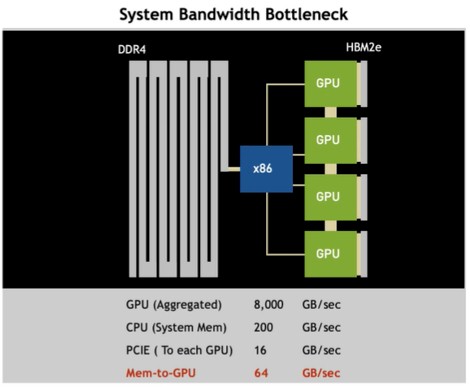
Here is what this Grace-Hopper module means architecturally. At the moment, when you have a hybrid CPU-GPU system, here is how the bandwidth all maps out:
And here is what happens on the Grace node with four CPUs and four GPUs:
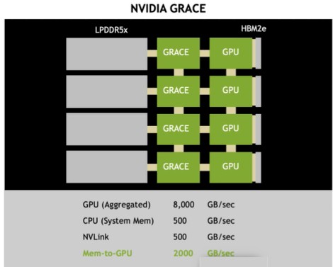
What these charts tell me is that Nvidia might be creating NVLink memory, with NVLink SerDes being linked directly to some kind of buffered memory, much as IBM is using its own signaling SerDes in Power10 chips as NUMA , I/O, and memory links.
Here is the upshot of this higher bandwidth hybrid node. Nvidia estimates that a Grace-Hopper system will offer 10X the performance on training natural language models, reducing it from one month to three days, and will allow for real-time inference on a 500 billion parameter model on a single node. And on the HPC front, computational fluid dynamics and weather applications are expected to see much-increased performance on the Grace-Hopper systems as well. Other HPC applications will no doubt follow.

The AI Wave Finally Starts Lifting Dell And HPE
It is beginning to look like the Dell Technologies and Hewlett Packard Enterprose, the world’s two biggest original equipment manufacturers, are finally going to start benefitting from the generative AI wave, mainly because they are finally getting enough allocations of GPUs from Nvidia and AMD that they can start addressing …
Arm CPUs To Take A Bite Out Of The HPC Market
Arm-based servers have had a somewhat checkered history that has seen many abortive attempts to challenge the X86 processor hegemony, but the firm appears bullish about its chances in the high performance computing (HPC) sector, where it believes its licensing model and the energy efficiency of its architecture give it …
Can Graviton Win A Three-Way Compute Race At AWS?
One of the main tenets of the hyperscalers and cloud builders is that they buy what they can and they only build what they must. And if they are building something from scratch – be it flash controllers using FPGAs a decade and a half ago or custom Arm processors …
the real time stock charts of NVDA AMD and INTC are fore telling
I’m guessing the 20 exaflops of AI performance for the Alps machine means fp16 tensor core performance, not general purpose fp16 performance. So if the next generation GPU architecture is similar to Ampere in terms of its tensor core acceleration factors, the linpack fp64 performance will be much lower, under an exaflops. NVIDIA calls Selene a 2.8 AI-exaflops machine, and its linpack RMax is 63.5 petaflops. If we multiply that by 7 times we arrive at a 444.5 petaflops machine.
Regarding the graphic NVIDIA provided that lists the memory bandwidths, it lists an aggregated GPU bandwidth of 8000 GB/s for 4 GPUs, or 2 TB/s per GPU, which is the same bandwidth as the 80GB version of the A100. I think HBM3 should potentially be along by the time of Ampere-next, but even if not, there should be a memory bandwidth boost for the chip using HBM2e. Presumably the listed aggregate GPU bandwidth is not really what they expect to see in the product.
Absolutely right. In my rush, I forgot about the TensorCores. . . .
The Denver-lineage of cores were still used in various Tegras until a few years back. Tegra X1, X2, used Denver follow-ons in mobile and Tegra Xavier used them in automotive.
>> Huang said that four Grace CPUs would deliver over 2,400 on the SPECrate2017_int_base test over four nodes, which means it is 600 per CPU.
That’s not what I heard in the Keynote. He said 2,400 SPECrate2017_int_base would be delivered over 8 nodes which tallies with the 300 SPECrate2017_int_base claim made about the throughput of a single Grace CPU.
What he said was actually weirder than I thought. I am getting further clarification.
>> 300 on the SPECrate2017_int_base test, which is on par with a 28-core “Skylake” and “Cascade Lake” Xeon SP processor from Intel.
I doubt the Cascade Lake Xeon SP performs that well on the SPECrate2017_int_base test. Please check the benchmark information at the URL below. The Xeon Platinum 8280 is one of the best performing CPUs of the Cascade Lake Xeon SP range and I think its score is more like 100, not 300.
https://www.anandtech.com/show/16594/intel-3rd-gen-xeon-scalable-review/6
I meant a pair of them. Test ranges, which I looked up, were around 350. For two, not one. Apologies.