

It would be convenient for everyone – chip makers and those who are running machine learning workloads – if training and inference could be done on the same device. For the moment, Nvidia has a virtual lock on machine learning training with its Tesla “Volta” GPU accelerators and it has made great inroads in the nascent inference space with its “Turing” GPUs, which are used in its most recent GeForce graphics cards as well as a low-voltage Tesla variant aimed at inference offload in servers.
At the recent Hot Chips 31 conference at Stanford University, we sat down with Bill Dally, who has headed up Nvidia Research for the past decade after a long and storied career at CalTech, MIT, and Stanford designing supercomputers and the interconnects that make them hum. Dally didn’t just write the book on interconnects, he actually co-authored three of them: Digital Systems Engineering (1998), Principles and Practices of Interconnection Networks (2004), and Digital Design: A Systems Approach (2012).
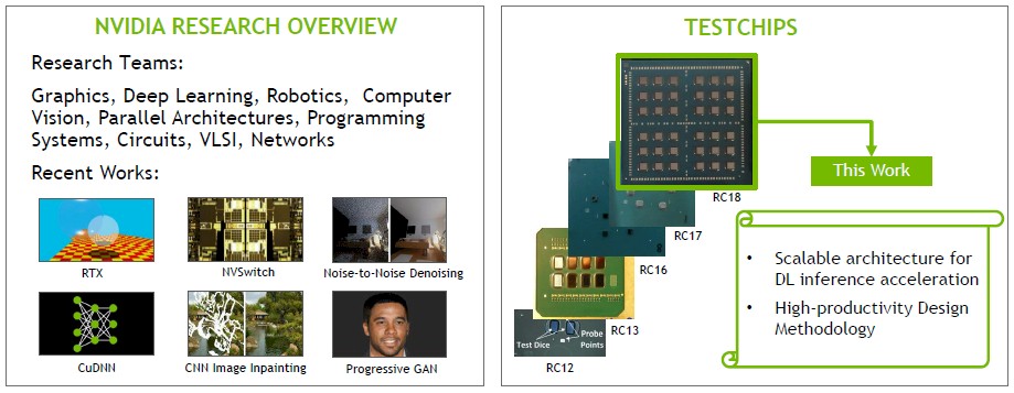
Ahead of the presentation of the RC18 research chip that Dally’s team put together last year and unveiled at the Hot Chips conference, we talked about chippery and interconnects and how Nvidia is loading up the shelf with technologies that are ready to be productized when the company needs them. After running through that chat, we will go over the details on the RC18 chip, which as Dally explains below, is interesting on many different fronts. This is a bit of an unconventional format for us, but these two things really belong in one place.
Timothy Prickett Morgan: So an inference chip that can chew through 128 teraops, that sounds like something that the market might need in the not too distant future as inference becomes an important, if not dominant, part of the software stack across companies of all shapes and sizes. Particularly one as energy efficient as the RC18 research chip that you are showing off. How close is this to being productized?
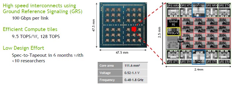
Bill Dally: We always do this. We have a whole bunch of technologies that we’re developing, but doing a chip is hard so we throw many of them together on a research chip to see how they play out. The RC18 chip is an efficient inference engine – it’s 9.5 teraops per watt, done in vanilla 16 nanometer process from TSMC.
TPM: That makes it around 13.5 watts, and that’s about as good as this is it going to get. And importantly, it is the kind of power profile and performance, and therefore power efficiency, that the hyperscalers and cloud builders are looking for in inference engines.
Bill Dally: The important thing is that we’ve demonstrated that anytime we want we can plop that into products. In fact, it can replace the Nvidia Deep Learning Accelerator. It’s actually designed very similarly to NVDLA, but we are as interested in the tools as much as we are about the chip. We developed the design space, exploration tools that try all combinations of vector widths, the number of vector units, the sizes of buffer arrays, and ways of tiling the loop to stage things. The tools came up with the optimal points for various neural networks.
TPM: Here is something we have been wondering about at The Next Platform as we look at all of these training and inference chips. What are the right sizes for the vectors? Google started with 256×256 in the TPU1 and then knocked that back to 128×128 in the TPU3, for instance. And the Nervana inference chips at Intel are 32×32. How do you decide the size of the matrix?
Bill Dally: The TPU is way too big. The ones we use in RC18 are 8×8. The way you decide is you take a bunch of different neural networks. You have this tradeoff because as you make it bigger it gets slightly more efficient on really big matrix multiplies but it gets less efficient when it doesn’t fit. If you make it really big, you amortize out the external overhead more but then if you can’t fill it you are just wasting space. As far as we are concerned, for inference, it’s somewhere between 8×8 and 16×16 – and it’s nice to make it powers of two because it makes everything map.
TPM: It’s a wonder that the TPU is so large, but they are also trying to do training and inference on the same chip. For inference, is the ideal matrix size likely to change?
Bill Dally: I don’t think so. If anything, some of the newer networks wind up wanting even a smaller granularity. I think we’ll push it more. I think it’s going to stay in the 8×8 to 16×16 range.
TPM: Tell us a bit about the different technologies that went into the RC18 test chip.
Bill Dally: One of the experiments we wanted to do was to figure out how to build a really efficient accelerator. We figured out that you waste power and timing margin by running everything off of one clock because you have to run the clock slow enough that the part of the chip with the lowest voltage can keep up with it. So what we do is we actually run each of our processing elements, or Pes, which are very small regions of the chip, on a separate clock which is locally generated and tracking the power supply. We have almost no margin, so we can run a frequency that’s right up to the hairy edge and then throttle back as the power supply dips.
But that means we have to synchronize as we move in and out of these relatively small regions. And so we created really fast synchronizers that do that do it on average in half a clock cycle. Normally, it’s like five or six clock cycles to go from one clock domain to another. This technology that won the best paper award at the International Symposium on Asynchronous Circuits and Systems (ASYNC) in May.
TPM: How do you do anything in half a clock cycle?
Bill Dally: It’s the average. Because the communication is asynchronous and only when you’re in that hairy region does it then delay you an additional clock to make it safe. But that almost never happens, so on average it ends up being a half clock cycle. So you really need the synchronizer technology that we’ve developed. And like the efficient neural network technology, it’s on a shelf so the product guys can pull it down anytime they want. It’s completely product ready, and it has been demonstrated in a realistic silicon, it’s ready to drop in there.
TPM: What kind of push do you have in getting them to productize something that you have created in the labs?
Bill Dally: Instead of pushing, we actually encourage them to pull. A lot of what I do is building relationships with people in other parts of the company and one of the tenets for how we run Nvidia Research is that technology transfer starts at the beginning of the project, not at the end.
TPM: That makes sense. But not every technology can make it.
Bill Dally: For all of these technologies, at the beginning of the project, we have this meeting where we identify who is the champion of and receiver for each technology. They’re often the same person, but in some cases they’re different people. And we start cultivating the champion at that point – the person who we need to trumpet this technology and get it into a product. And sometimes they pull things out of our hands before we are precisely ready. NVSwitch was that way. We were developing NVSwitch in Nvidia Research and we wanted to play with a little bit more, but they came in and said – whomp! – this is a product.
TPM: It sure looks like they were right, looking at DGX-2 and all of its clones.
Shifting topics, there is a lot of pressure on inference these days, and the competition is really good on inference. . . .
Bill Dally: Well, they like to say they are.
TPM: Well, the competition is relatively strong, at least compared to training, which is pretty weak compared to Nvidia GPUs. And ignoring the fact that many of the inference upstarts don’t have fully developed software stacks, you’ve got to admit that the inference players have got a better shot at taking market share away from Nvidia and, perhaps more significantly, taking share away from Intel’s CPUs, which still do most of the inference in the datacenter these days.
Bill Dally: Inference is more of a greenfield because there’s no dominant player yet the way training has got a dominant player. But you know what? We have great discussions with the people who are designing the next generation GPUs, which right now actually means two GPUs after Turing because the one after Turing is done. And they understand what we’re doing and we understand what they are doing.
TPM: Do you have code names for these GPUs? [Laughter]
Bill Dally: I don’t think we’ve publicly released code names. And so you know we are we are very strongly influencing what they’re going to do. They understand what we’re doing. We have weekly meetings with these guys so that the technology is transferred in the sense that they’re involved from the beginning of our project. They know what we’re doing they can grab it anytime they want and move it over. That goes for the efficient accelerator, it goes for the synchronizer.
We also are demonstrating a multi-chip module on an organic substrate using a signaling technology called ground-referenced signaling. GRS is single ended and, unlike the differential signaling technology commonly used today, it gives you twice the bandwidth per pin and, more importantly, twice the bandwidth per millimeter of chip edge. This is key because that’s actually the scarce resource – you can put more pins on, but you got to squeeze all the wires out from under the edge of the chip.
TPM: Understood. Now I have to learn a new networking scheme. Thanks for that.
Bill Dally: And GRS is 25 Gb/sec, so that means it’s equivalent to a 50 Gb/sec differential technology in terms of bandwidth. And it runs at 1 picojoule per bit moved, so it’s about a factor of seven better than the average 25 Gb/sec SERDES, which runs at 7 picojoules per bit. And it’s just wonderful for connecting things in an organic substrate. That’s how we’re able to scale this inference accelerator from one chip to 36 chips transparently. So that’s a technology that’s on the shelf. And there’s a couple other technologies that are in there. But the whole point of the chip is basically to demonstrate and de-risk technologies so they can go on the shelf and product developers can use them with confidence.
As I hinted at previously, another really key technology focused on design methodology. The whole RC18 chip was designed by fewer than ten engineers in six months, coded entirely in C++ using high level synthesis. If you look at the NVDLA chip, which is a very comparable design in terms of complexity, RC18 had about an order magnitude less design effort with a comparable quality of design. And so we’re basically developing new design methods will make it faster for us to design almost anything.
TPM: That’s pretty cool.
Bill Dally: It is very cool. Don’t tell Jensen this, but I would probably do what I do if he didn’t pay me because it is so much fun.
TPM: Too late. You’re on the record. Good thing you qualified that with “probably.”
And now, let’s take a look at that RC18 test chip, which might portend some of the future of Nvidia’s GPU designs. Or not. This is not a GPU, and it could be commercialized more or less as is.
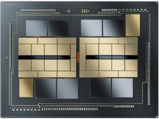
The RC18 has a tile approach to building up the compute, just as several of the prior RC classes of chips did, and this one adds in distributed memory across the tiles. Here’s how the compute elements are built up hierarchically, starting with the processing elements, which are in the zoom below:
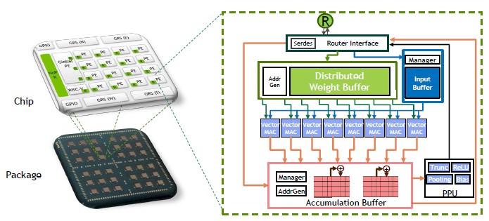
Each processor element, or PE, has eight vector multiply accumulate (MAC) units; there are 16 of these Pes on a chip, plus a global PE and a single RISC-V core for handling serial functions and I/O – let that be a warning to you, Arm Holdings. The PEs can process a total of 64 8-bit multiply-accumulate operations per cycle, and across the 16 computing PEs on the chip, that’s 1,024 operations per cycle per chip. With 36 chips on the die, that’s a total of 36,864 operations per cycle.
Data comes in to each PE over a router interface, with a distributed weight buffer and an input buffer front-ending the vector MACs. As data pours through the chip, it feeds into an accumulative buffer, which in turn feeds back out into the mesh network linking the cores to each other. The routers on each PE implement a 4×5 mesh topology on the chip, and it takes about 10 nanoseconds per hop with the mesh lanes able to deliver around 70 Gb/sec of bandwidth at 0.72 volts. At that voltage, the routers are clocking in at 1.1 GHz; depending on the voltage applied, the clocks on the PEs scale from 480 MHz to 1.8 GHz.
On the package, the 36 chips are hooked into a 6×6 mesh topology, with each chip having its own router chip with four interfaces to the higher-level mesh. The routing is configurable so it can heal around bad links or dead chips, which means such failures do not take out an entire processing complex. The latency of a hop across this network on package mesh is around 20 nanoseconds and the links run at a maximum of 100 Gb/sec. The inter-chip interconnect is what is based on the GRS technology that Dally was talking about above.
So very generally, here is how it works. The system uploads the weights created by a machine learning training model into the registers on each PE. The input activations for the inference are added to the Global PE, and then the RISC-V processor configures the control registers. The input activations are streamed down into the PEs, and then the output activations are pushed back into the Global PE. Data can be synchronized and spread across the multiple chips in the RC18 device to scale across the 36 tiles on the RC18 package.
As you might imagine, the more cores that are activated, the more energy those mesh networks consume on an RC18 chip to crosstalk as inference is performed.
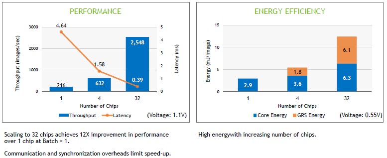
On the ResNet-50 image recognition benchmark test, with a batch size of one (meaning images were inferred in series as they came into the chip rather than being batched up into bundles of 10 or 25 or 100 as is commonly done on larger inference engines to boost their throughput), the RC18 was able to process just under 2,500 images per second with a 390 microsecond latency across 32 cores. That’s very good latency, and pretty good performance for such a small device. But that performance comes at an energy cost, as it always does. It doesn’t take long before the GRS signaling between the chiplets on the RC18 package consume as much power as the cores themselves when running an inference.
From this, we posit that not only is time proportional to money, but energy is inversely proportional to time. So if you have more time, you can burn less energy. That’s true of just about every kind of machine ever invented because, physics.

Nvidia Picks Up The Pace For Datacenter Roadmaps
Heaven forbid that we take a few days of downtime. When we were not looking – and forcing ourselves to not look at any IT news because we have other things going on – that is the moment when Nvidia decides to put out a financial presentation that embeds a …

A Peek Into The Future Of AI Inference At Nvidia
The best kinds of research are those that test new ideas and that also lead to practical innovations in real products. It takes a keen eye to differentiate science projects, which can be fun but which can also lead nowhere, from useful stuff. At Nvidia, the job of steering research …
The Year Ahead In Datacenter Compute
For more than a decade, the pace of the server market was set by the rollout of Intel’s Xeon processors each year. To be sure, Intel did not always roll out new chips like clockwork, on a predictable and more or less annual cadence as the big datacenter operators like. …
2020 chip has been done. 7nm Nvidia chip will prove once again Nvidia is one generation a head