

The rise of public and private clouds, the growth of the Internet of Things, the proliferation of mobile devices and the massive amounts of data that need to be collected, stored, moved and analyzed that are being generated by such fast-growing emerging trends promise to drive significant changes in both software and hardware development in the coming years.
Depending on who you’re talking to, there could be anywhere from 10 billion to 25 billion connected devices worldwide, self-driving cars are expected to rapidly grow in use in the next decade and corporate data is no longer housed primarily in stationary storage appliances in the datacenter, but are accessible via cloud environments, mobile devices and IoT devices.
For hardware makers, the push is on to create servers and other systems that can move out toward the edge of the corporate networks, to be as close as possible to the sources of the data to ensure near-real-time analysis of the data and to reduce the amount of traffic going over the networks by determining at the point where the data is generated which information needs to be routed back to the datacenter and which is irrelevant and can be deleted. There is increasing demand for smaller, more energy-efficient and more powerful compute systems that can be placed out at the network’s edge or in the end devices themselves, such as automated vehicles.
That in turn will demand not only new materials for the compute systems but also new ways of packaging the components to ensure high density, high performance and energy efficiency, according to Shigenori Aoki, who leads R&D on devices, hardware implementations and new materials at Fujitsu Laboratories. In recent research, Aoki talked about some of the research work that Fujitsu Labs is doing in terms of developing technologies and processes for an increasingly hyperconnected, cloud-centric world. The work includes not only such new materials as nanocarbon for carbon-based semiconductors but also new capabilities like extra-sensitive sensors.
Fujitsu engineers also are focusing on developing new ways of packaging components to create information and communications technologies (ICT) to handle the demands of the IoT era in which the data traffic on networks will jump 23 percent in the coming years but will have to be moved and managed on systems that can’t grow in size or consume more power than current hardware, he wrote. He also envisions a future where systems like autonomous vehicles will need to carry essentially small, compact and powerful servers inside of them, and HPC systems small enough to carry. Aoki’s idea of a device packaging roadmap for primarily server applications looks like this:
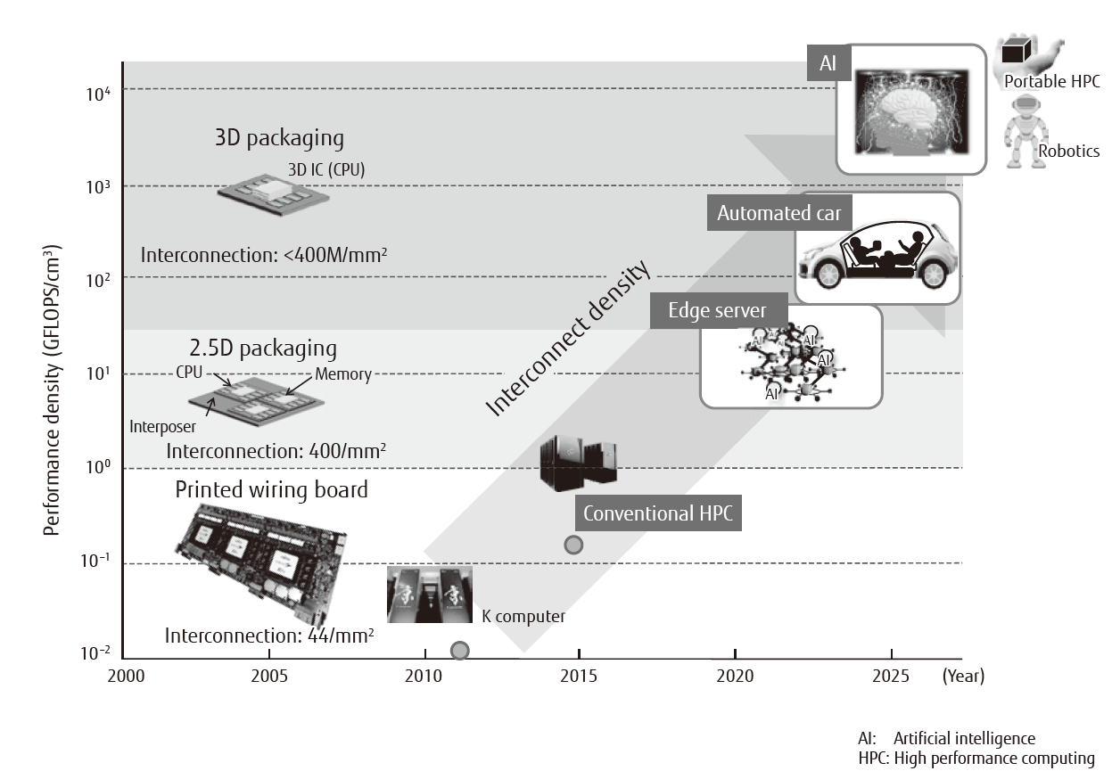
In the past, many of the improvements in hardware have been tied to the shrinking of processors and other components. However, that trend – driven in large part over the past five decades by Moore’s Law – is slowing, forcing hardware makers like Fujistu and others to consider other parts of the equation, such as packaging.
“In a few decades, semiconductor devices and related hardware have led ICT progress with downsizing, cost-cutting, and upgrading,” Aoki wrote. “The scaling of silicon MOS devices and the following packaging development has miniaturized supercomputers in the twentieth century into today’s smartphones. “Silicon scaling has been slowing down since 2010, because of physical limitations in processing technology and difficulties related to the huge [financial] capital expenditure that is required. This financial aspect reduced the number of silicon MOS vendors, so that only a few companies now survive in areas of processors, DRAMs, and so on.”
According to Aoki, “where there is uniformity between core devices, original packaging technologies come to be essential.”
For high-density packaging, a key is reducing the length of wiring between devices to reduce latency and overall device size. Currently, much of that has translated into fine wiring lines on a substrate close to semiconductor devices. Such wiring lines are expensive and for the most part have been used in such high-end systems as supercomputers. However, the growing demand for compact and powerful servers for such systems as self-driving cars is calling for systems that have the performance of a high-end server rack but that a tenth to a hundredth of the size. Fujitsu is developing the use of 2.5-dimension integrated circuits – interposers made from a silicon substrate developed via a semiconductor-class process that Aoki said results in more dense wiring and products about the tenth of the size of current systems. The 3D process of stacking silicon wafers and dies and interconnecting them vertically can bring more density by a factor of 100, but the process is expensive. For small, dense servers to find their way into cars and the network edge, a less expensive process will be necessary, he said.
“Future neuro-computers and brain-type computers need a great number of interconnects between processors, and the number is an order of magnitude larger than today’s one,” Aoki wrote. “At that time, a novel higher-density packaging technology will appear based on the current 3D ICs.”
Fujitsu also is pushing ahead with research into silicon photonics. As we’ve talked about before at The Next Platform, as the challenges of shrinking transistors to keep pace with Moore’s Law become apparent, chip makers are looking at other ways to keep the performance gains going. Moving data more quickly and efficiently is one of those ways, and silicon photonics has been getting a hard look for years from the likes of Intel, IBM, Mellanox and Juniper Networks. It promises lower power requirements and better transmission distance when compared to copper-based I/O technologies. Fujitsu Labs also is developing silicon photonics technologies, including with narrow-space optical wiring, where silicon optical waveguides “strongly confine light and turn it with much smaller diameter than the conventional glass waveguides,” Aoki wrote.
Cooling is another aspect of packaging that Fujitsu engineers are focusing on. In particular, they are looking to take the water-cooling technology they’ve developed for large-scale systems like the K supercomputer – currently number seven on the Top500 list of the world’s fastest systems and powered by 705,024 SPARC64 VIIIfx processing cores – and bringing it to smaller high-density packages. Technologies like as 3D ICs and silicon photonics will need new cooling technologies aimed at hot spots within the integrated circuits. Moving a coolant through such a small space is not easy, given issues around flow rate, pumping power and the small size of the channels, but Fujitsu has developed a two-phase cooling system that uses coolant vaporization, which Aoki said needs a slower flow rate than liquid cooling and enables the self-circulation of the coolant in a manner similar to heat pipes. Aoki said the plan is to bring the cooling technology to both computers and mobile devices.

Fujitsu To Fork Arm Server Chip Line To Chase Clouds
When it comes to chips, there is a big difference between a kicker and a fork. The kicker is a successor that implements an architecture and design and that includes microarchitecture enhancements to boost core performance (core in the dual meanings of that word when it comes to CPUs) as …

A Five-Year Challenge Roadmap for Photonics-Based Computing
Silicon photonics has been proving its worth in telco and communications but there is a much brighter opportunity photonics-based computing. The energy efficiency and data movement potential is promising, especially for increasingly data-laden analytics and AI/ML applications, but the road to a diverse hardware ecosystem for compute is still long. …
Fugaku Remakes Exascale Computing In Its Own Image
When originally conceived, Japan’s Post-K supercomputer was supposed to be the country’s first exascale system. Developed by Fujitsu and the RIKEN Center for Computational Science, the system, now known as Fugaku, is designed to be two orders of magnitude faster than its predecessor, the 11.3-petaflops (peak) K computer. But a …
Be the first to comment