As we pointed out in the analysis opening up this series on the future prospects for ARM-based servers, it has been quite a challenge getting all of the hardware, software, and money lined up to storm the datacenter. It is tough enough to bring a new architecture into the datacenter, but doing so against Intel, which rules compute and storage these days and has a growing influence in networking, is quite another matter.
By contrast, the minicomputer pioneers four decades ago had it easy when they attacked the datacenter because the mainframe giants of the time lived in their ivory fortresses and did not understand the forces lapping at their ramparts, eroding them. (One of those minicomputer innovators was none other than Britain’s Acorn Computers, which formed a chip development partnership with Apple and VLSI Technology that lives on today as ARM Holdings.) The mainframe and minicomputer giants a decade later were in denial about the RISC/Unix system revolution that laid the foundation for the commercial Internet, and that gave Sun Microsystems, Hewlett-Packard, Data General, and time to build up a very large and profitable business selling these new architectures against the incumbents.
The ARM insurgents find themselves up against not only each other, but an Intel that has dominant market share and has effectively vanquished AMD’s Opterons X86 processors from the datacenter and would have made it exceedingly tough for the company to break back into the glass house with either X86 or ARM chips no matter what. AMD no doubt stumbled badly with its “Barcelona” Opteron bug at the same time the Great Recession was starting and that Intel had put together its competitive (and we would say Opteron-inspired) “Nehalem” Xeon 5500 architecture. AMD lost its key partnership with supercomputer maker Cray, which had tightly coupled its “SeaStar” and “Gemini” clustering interconnects to AMD’s HyperTransport point-to-point interconnect on its Opterons, and now Cray is very tightly aligned to Intel, which interestingly bought the Cray interconnect business for $140 million in 2012 and took on the key developers behind this advanced technology. (In a sense, the impending Omni-Path interconnect is what happens when you take the best ideas from QLogic InfiniBand, which Intel bought at around the same time, and Cray Aries interconnects and move them forward.)
Here we are, ten years after the peak of enthusiasm for Opteron in the datacenter, which was driven not just by enterprises but also by companies such as Google, Amazon, Microsoft, Rackspace Hosting, and others who were pushing from scale into hyperscale at the same time. The difficultly for AMD throughout the go-go years for the Opteron, when it had 64-bit processing and multicore ahead of Intel’s Xeon processors and garnered an incredible 25 percent market share in certain segments of the X86 server space, was getting customers to admit they were using Opteron chips. These processors were of such strategic advantage that the newly hyperscaling as well as large enterprises and service providers that had broadly adopted Opterons were reluctant to admit it. And in a few short years, with Opteron delays and glitches, the air basically came out of AMD’s server business. Buying microserver upstart SeaMicro in early 2012 gave AMD a chance to tackle a new market and a potential interconnect to bring to bring to bear against Intel, but that did not pan out and AMD wrote off the SeaMicro investment this past April.
AMD has seen a resurgence of sorts thanks to its taking over as the supplier of processing and graphics for game console makers Microsoft and Sony, who formerly used chips from IBM as the engines in these machines. The declining PC business has not done AMD any favors, and its lack of a sizeable presence in servers hurts, too, on both the top and bottom lines. All of the ARM chip makers want to get into servers because they think they can extract profits. But we think it is far more likely that if ARM server chips get a foothold in the datacenter, it will be after a particularly bloody price war that will put a serious dent in the last bastion of profit in the X86 server space: The very impressive margins of Intel’s Data Center Group.
ARM chip makers will have to compete on price as well as performance and thermals, and the laws of physics are going to run hard up against the laws of economics. What we can tell you is that customers will win, for sure, because of the indirect pressure that Intel feels from ARM, Power, GPU, and other architectures as well as any direct competitive pressure.
We think AMD’s past as the provider of components to both HPC centers and hyperscalers is experience that other ARM contenders cannot claim to have, and its experience as a provider of components used by enterprise system makers in the 2000s is not to be underestimated, either. It is reasonable to consider how many of its system experts are still working at AMD, and it is also reasonable to contemplate why Jim Keller, the architect of AMD’s “Sledgehammer” K8 architecture that brought us the Opteron in the datacenter, left AMD after working on the future “K12” ARM and “Zen” Opteron processors for the past three years. As AMD pointed out to The Next Platform, Keller is one of the luminaries of the chip industry and he tends to take on projects for a few years – like working at PowerPC startup PA Semi a decade ago and then moving to Apple when the consumer electronics behemoth bought PA Semi to help design Apple’s A4 and A5 ARM-based processors – that interest him.
Read into it what you will, and even if you assume that at this point most of the design work for the ARM K12 and the Opteron Zen processors is largely complete, AMD no doubt would have preferred that Keller stick around and help drive chip designs further out. One could also make the case that Keller would have helped AMD better sustain its Opteron advantage a decade ago, too.
Redrawing The Roadmaps As The Terrain Changes
You would have thought that AMD’s “Project SkyBridge” plan to deliver a unified socket for ARM and Opteron processors would have resonated well with system makers, hyperscalers, and maybe even HPC shops. SkyBridge was about more than sockets. It was a way to take blocks of circuits implementing accelerator interconnects, network fabrics, and other chip features and making them common across X86 and ARM architectures. (Cavium Networks and Broadcom are doing the same with their MIPS-based processors as they craft ARM chips, so this idea is not new.)
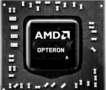
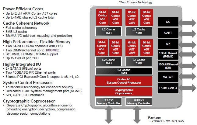
In May 2014, when AMD provided its server roadmap update and first announced that Keller had been working at AMD, the “Seattle” Opteron A1100 based on ARM Holding’s Cortex-A57 cores was sampling. The Seattle chips are etched in 28 nanometer processes by GlobalFoundries, and AMD was expecting to shrink down to 20 nanometers with a SkyBridge-compatible chip using low-power Cortex-A57 cores in 2015. The future ARM K12 chips, based on a customized variant of the ARMv8-A architecture, were expected in 2016, and while AMD never said what process might be used, it would have to 14 nanometers to be ground-breaking.
Clearly, getting a common socket is not what potential AMD server chip customers have said is that they want a real alternative to Intel Xeon and Atoms and this is more important than having a platform that supports AMD ARM and Opteron chips. We also think that potential hyperscale and HPC customers – the ones that will potentially be the early adopters of the future Zen server chips – have been explicit that they want a situation like they had a decade ago, where the competition was fierce between AMD and Intel on the X86 front.
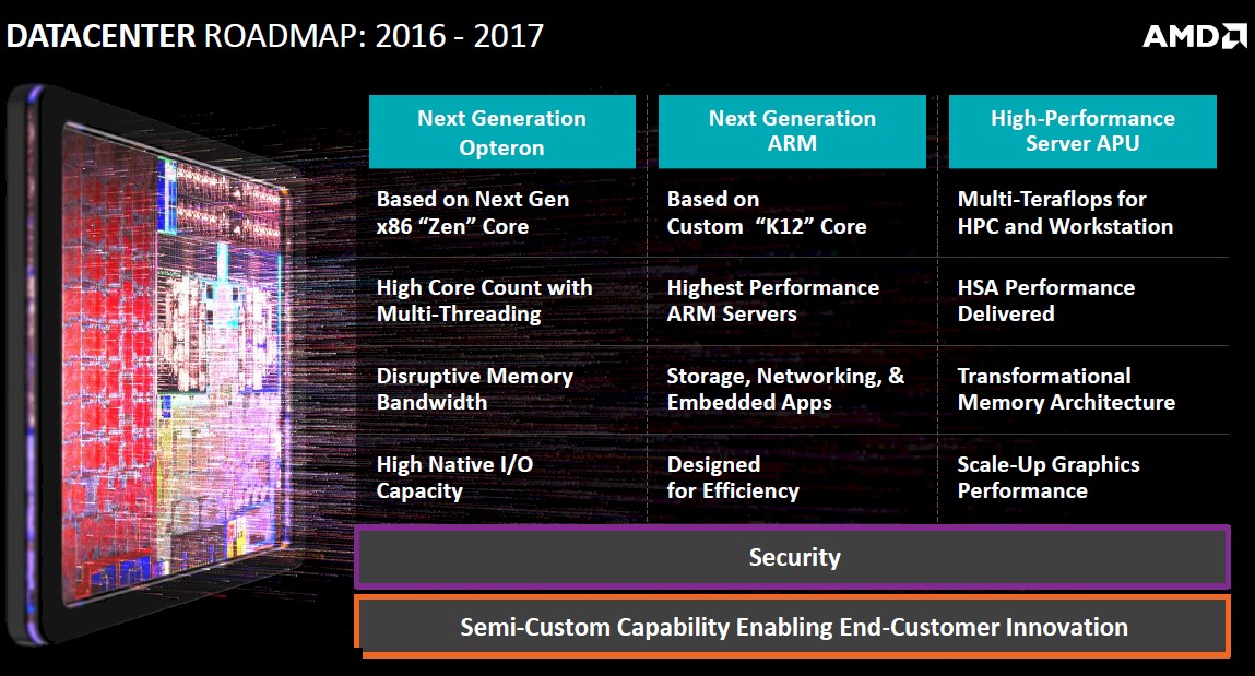
And so, back at its financial analyst’s day in July, SkyBridge was put out to pasture and so was the idea that AMD’s ARM and X86 processors would be developed side by side for both system-on-chip (SoC) and Accelerated Processing Unit (APU) hybrids, which put CPUs and GPUs on the same die. Now, everything at AMD is focused on getting the Zen Opterons to market in 2016, based on a 3D transistor FinFET processor that AMD has not specified and from a supplier it has also not specified. (It has to be either GlobalFoundries or Taiwan Semiconductor Manufacturing Corp, the two foundries that AMD has used since buying graphics chip maker ATI Technologies in 2006 for $5.4 billion.) Now, the K12 chips follow Zen-based Opterons in 2017 and an unspecified “high performance server APU” is also expected in the 2016 to 2017 timeframe, and if the roadmap is linear, then it is in 2017.
AMD has also done some very interesting work on exascale systems, but it is not at all clear how the insights that the company has researched will be productized, and who would fund that further research and development.
The target that Forrest Norrod, general manager of the AMD’s Enterprise, Embedded, and Semi-Custom Business Group and formerly general manager of Dell’s systems business, is aiming at is not small. Back in July, Norrod said that AMD believed the market for server chips was about $10 billion a year, with another $4 billion (and perhaps more) used in networking devices that are shifting from proprietary ASICs to software running on X86 or ARM processors. AMD thinks there is another $2 billion or more in the software-defined storage market. That adds up to a $16 billion target. Getting even a modest piece of this would turn AMD around.
How To Get There From Here
So here we are at the end of 2015, and the Seattle Opteron A1100 ARM-based chips are about a year late to market and the K12 chips have been sampling in the labs since July and AMD has said that the launch of K12 chips will be timed to coincide with the maturity of the software stack for 64-bit ARM server chips. The good news for AMD is that other ARM chip vendors are having their own issues getting chips to market and getting design wins for the chips in systems, storage servers, and other devices in the datacenter, too.
Without performance figures or pricing information for the Seattle chip, it is hard to make a comparison to any X86 processor, whether it comes from Intel or AMD itself. The Seattle chip was designed to have its eight A57 cores running at 2 GHz or higher, and with up to 128 GB of main memory – twice the cores and twice the memory of the four-core Xeon E3 server chips from Intel, and so by design. The idea was to have twice as many cores and twice the memory, and have slightly more performance. The only problem is that the feeds and speeds of the Seattle chips have been known since mid-2013 and started sampling in March 2014 should have beat the Xeon D processor launched by Intel this past March to market by about a year. And now, it looks like Intel is beating Seattle to market with the Xeon D.
The Xeon D is the first Xeon based on the “Broadwell” core and has eight cores and two memory controllers with two DIMMs per channel – just like Seattle – and supports up to 128 GB of memory – just like Seattle. It also has two 10 Gb/sec Ethernet ports and six SATA ports – just like Seattle. The Ethernet controllers are on the die, and Intel southbridge for legacy I/O controllers is in the same package, offering the same small footprint as AMD was promising with the Seattle. The Xeon D-1540 comes with eight cores running at 2 GHz and has a thermal design point of 45 watts; it costs $581; the Xeon D-1520 has four cores running at 2.2 GHz, and costs a mere $199 and burns only 20 watts. And there is little question that Facebook will be using the Xeon D in its “Yosemite” microserver designs – servers that can take Seattle chips and might if Facebook is feeling ambidextrous.
Still, it is fair to say that AMD left Intel too much room and too much time to come up with an answer to Seattle. (This is why Broadcom and Qualcomm have said very little about their respective future “Vulcan” and “Hydra” ARM server chips.) No one needs to school AMD about this – they smashed the Xeon server business wide open with SledgeHammer when Intel left a hole by being stubborn about 64-bit addressing on Xeons back in the early 2000s.
AMD has not said why Seattle is so far behind schedule, and we cannot venture a guess. But we will point out that the company no doubt would have like to have shipped Seattle a year ago and was probably stymied by the evolving ARM software stack – issues Intel does not have to cope with on the Xeon D since it is a Xeon processor and can run Windows, Linux, FreeBSD, and so forth. It is possible that the chip itself has had problems, too, but no one is saying.
“I continue to believe ARM has a place in the datacenter as you think about the convergence between networking, storage, and servers,” explained AMD CEO Lisa Su in a conference call a few weeks ago going over AMD’s financial results for the third quarter. “I think it is fair to say for all of us that it has been slower to adopt in the server market just due to the some of the software and the infrastructure. Relative to Seattle, we will be starting our first modest production shipments in the fourth quarter in this coming quarter this year. I view it as a longer-term bet, so no question that server market is attractive, datacenter is attractive. But we are very focused on it from an X86 standpoint and we will continue our ARM efforts in a complementary way.”
Michael Detwiler, product marketing manager for the Seattle chip at AMD, spoke to The Next Platform and said that AMD is working to get the chip out the door and that it has two design wins so far. The first is for a reference system being put together by the Linaro “Linux on ARM” software development effort, which will use a four-core variant of Seattle to create a basic box for programmers to play with; it will use SODIMM memory to bring the cost down, and will support CentOS, Fedora, and Red Hat Enterprise Linux Server for ARM Development Preview editions of Linux. British server maker SoftIron has created a 1U rack-mounted, half-depth server called the Overdrive 3000 that has an eight-core Seattle chip configured with 16 GB of base memory, openSUSE Linux, and a GNU compiler stack. The clock speed on the chip is not divulged, and neither is the price. But the Overdrive 3000 is aimed at developers and is not intended for production.
We have said it before and we will say it again: An ARM server chip cannot get traction until Red Hat Enterprise Linux (the real and full one), SUSE Linux Enterprise Server, and Canonical Ubuntu Server are certified to run on it. If there was widely available iron, it sure would help them out.
Detwiler says that there are a number of other wins with Seattle, but that he cannot talk about them. But he did tell The Next Platform what markets AMD is aiming at with the processor.
“At a high level, where we are targeting and where we are getting the most traction is software-defined storage, and I am thinking in particular of the cold storage variety of where you don’t need a whole lot of compute capability and it is not about core performance, but you do want low power and there are advantages for high levels of integration,” Detwiler explains. Seattle is also being pitched as a platform for content delivery networks and hosting, and software ecosystem development. The latter one is important, he adds. “ARM doesn’t have a chance to be successful if you don’t make it look and feel like X86. This is a barrier to adoption, and you have to make this look like a server that the typical IT person has used for the past twenty years. The idea is to push the software development, but at the same time there is enough of the software ecosystem available today – the LAMP runs fine on ARM – that we can have some key wins early on while we are pushing the ecosystem and getting ready for the next-generation of ARM processors.”
Detwiler confirmed that AMD is still developing K12 and that has not changed. The first Opteron Zen chips – of which AMD has said very little – are close to taping out and despite Keller’s departure (now that the bulk of the design work for Zen and K12 are done), AMD has a deep enough bench to carry on with the work. AMD is going to use the unnamed 3D transistor FinFET process on its future GPUs first next year, and then it will be applied to Zen-based Opterons. The important thing is that AMD and its fab partner will have some experience on the FinFET manufacturing process before it is deployed on Zen Opterons.
With Seattle being met by the Xeon D, the obvious question is what is the design goal of the K12 Opteron chip, which is coming to market around a year and a half to two years from now – if all goes well. That is a lot of time to give Intel, which will be shipping “Skylake” Xeon E5s around then, which we told you all about here.
“Think of this as being higher performing,” said Detwiler, referring to the K12 core and the as-yet unnamed future Opteron A series chips that will make use of it. “That would be the reason we would do a design in the first place, and I can’t get into the complete strategy, but the idea is to have the highest performing ARM server chips.” When we pressed about whether this meant both single-threaded as well as throughput performance, Detwiler said this was accurate and compared to the approach that AMD was taking with the Zen cores on the X86 side of the Opteron lineup.
The simplest thing for Keller and his team to have done is to create a basic shell of a processor, with caches and on-chip controllers for memory and I/O and acceleration and then have one flavor using Zen cores and another one using K12 cores. This can be done without having the pinouts and sockets be the same, of course, and allow for certain blocks – such as those for NUMA clustering – to be removed from the ARM chips if that is desirable. (There are lots of ways to skin this cat.) What is clear is that to meet the 28-core Skylake chip on the field of battle in the datacenter, AMD will have to wield a pretty hefty Zen Opteron chip for desktops and possibly servers in 2016, and that could lead to a similarly hefty K12 chip in 2017.
We have seen the rumors about the Zen-based Opteron chip with an integrated GPU, what looks like the HPC-focused APU that AMD has on its roadmaps but which AMD has not confirmed. This is a very sweet looking chip, but one AMD needs to be selling last year, not next year. The rumors suggest that this APU will have 16 Zen cores with 32 threads, and pack 512 KB of L2 cache per core and have a 32 MB shared L3 cache across those cores. This unnamed Zen Opteron will also have a “Greenland” family stream processor and up to 16 GB of HBM that delivers 512 GB/sec of memory bandwidth. For more memory expansion, this Zen Opteron will have four DDR4 memory controllers, and it will also pack in 64 lanes of PCI-Express 3.0 I/O.
If that is the APU, what about a plain CPU? Well, kick out the GPU and perhaps add another dozen cores and you have a Zen Opteron with 28 cores and 56 threads – exactly what Intel is delivering with top-end Skylake Xeon E5 v5 processors, if that plan doesn’t change.
It would be very interesting indeed to see if the ARM Opterons from AMD could keep core pace and it could deliver an APU with 16 K12 cores, a streaming GPU, and a big chunk of HBM for killer memory bandwidth, and then a K12-based CPU with our hypothetical suggested 28 cores and no GPU but maybe keep the HBM.
We think that AMD will try to do beefy rather than skinny cores, and try to get each core to crank faster to get decent single-thread performance as well as overall throughput. The question – and one no one has answered yet – is just how much work would a very beefy ARMv8 core do compared to a Xeon core? AMD could do what IBM and Oracle do with their respective Power and Sparc chips, which is have beefy cores run at a relatively high clock speed with dynamic threading that allows two, four, or eight threads per core when workloads can make use of them and one thread per core when the job is not really well threaded. If that Zen APU slide is real, AMD is delivering two threads per core, but it may need more than that.
Whatever AMD does, the main thing is that it can’t hide and keeping its future secret is not helping as much as the company’s management thinks. With AMD’s revenues sliding, the company announcing layoffs, persistent rumors that it is for sale (no, Qualcomm is not going to buy AMD), and a $371 million deal to sell off its chip assembly and test operations, what AMD needs to do is show its commitment to its processing future.
That means putting a stake in the ground, like Oracle did when it bought Sun Microsystems, or like IBM did recently with its OpenPower partners, and giving customers a roadmap. If that AMD X86 and ARM roadmap can’t match up against what Intel is already saying it can do, that is the real problem. Telling people about it is not.



The Big question for AMD’s K12 is did Jim Keller bake SMT ability into its Custom ARM cores! There were a lot of YouTube interviews with Keller basically indicating that there was a lot of cross sharing of design ideas among the Zen and K12 design teams. So do both Zen and K12 share the same core design tenets and is it just that they are made to execute their respective ISAs. These K12s may be the first custom ARMv8a ISA designs than have SMT, and it will be the custom micro-architectures that are engineered to run the ARMv8a ISA that will make the server market interesting and not so much the Arm Holdings’ reference designs. ARM is a RISC design, but so is Power8, so what is stopping a Jim Keller from taking a custom ARM core and making it an extra wide order superscalar design like the power8 at some point in time. K12 because it’s a RISC design will be able to support more cores with greater SMT threads per core per unit area, like Power8. So just what may be in store once the Zen products are released to market and AMD can begin to focus on K12. AMD has stuttered SeaMicro but that freedom fabric IP is still in AMD’s possession, along with other SeaMicro IP.
Those Greenland based HPC APU’s should be using HBM2 at double the bandwidth and memory per stack than HBM, and the Greenland GPU micro-architecture will be brand new. Just what new asynchronous compute ability has AMD’s GPU division baked into the ACE units on the Greenland micro-architecture. AMD’s GCN ACE units can context switch both compute and graphics threads at the same time with very little under-utilization of GPU processing resources, while Nvidia has to do with an inefficient software implementation that does not fully implement true hardware based asynchronous compute ability. AMD may become a much in demand supplier of GPU acceleration parts, especially if it takes the Freedom Fabric IP/other IP and implements it like it has demonstrated for its exascale Grant proposal using the APU CPU/GPU on an interposer design with a fully coherent connection fabric. Add to that AMD’s recent patent filings for FPGA’s added to the HBM stack for some in HBM memory FPGA compute sandwiched between the bottom HBM memory logic/controller die and the HBM dies above. With silicon interposers AMD can potentially connect up CPU cores to GPUs with uber wide parallel traces in the very same manner that GPU processors are wired up to HBM on AMD’s latest GPU SKUs. We are talking about thousands of traces between CPU and GPU, in addition to those wide traces to the HBM stacks, with low power saving clocks and high effective bandwidth for both memory channels and CPU to GPU on interposer interconnects, a big plus for HPC and exascale computing.
The problem with AMD is since 10 years its execution which has been terrible no matter who sits on the top of the company. Also there seems to be no coherrent strategy. SeaMicro was a great chance totally blustered by the upper management. In a game that becomes more and more expansive you can’t allow that to happen anymore. One more bad execution and AMD is gone for sure
SeaMicro being shuttered is AMD’s former CEO(Rory Reed) trying to bite of more than AMD had the financial ability to chew on! But AMD still has the SeaMicro IP, and some of that IP will find/has found its way into AMD’s HPC/workstation and exascale products. That SeaMicro Freedom fabric, and other IP still has potential in AMD’s future road-maps. AMD has to get Zen to market and producing revenues, and Zen is on schedule and samples are performing up to expectations if the latest news is correct. AMD’s GPUs are closing the gap with Nvidia’s offerings, and with the latest driver updates AMD’s current offerings are even beginning to surpass Nvidia’s offerings.
AMD’s GPU’s fully in hardware asynchronous compute abilities will have HPC/workstation and exascale computing implications against Nvidia’s GPUs! Nvidia’s current crop of GPUs do not posses the ability in their GPU hardware to schedule asynchronous compute threads on its GPU processor’s execution units! Nvidia has to rely on inefficient software scheduling for its GPUs, and this results in idle processing units that have to wait on inefficient software based thread dispatching, which results in wasting GPU cycles. AMD’s ACE units and their fully implemented in hardware asynchronous compute has already shown an advantage on non graphics gaming workloads, as well as gaming graphics workloads with DX12, Vulkan, with AMD able to accelerate more than just graphics for gaming, and non gaming software applications. The VR folks are betting on AMD for that very reason, and Nvidia better get some fully hardware based asynchronous compute abilities or be behind!
A short read-up on AMD’s proposed exascale solutions have AMD providing an HPC APU On An Interposer sharing with 16/32 Zen cores with a full Greenland GPU(New Arctic Islands GPU micro-architecture ISA) accelerator, and adds to that some FPGA power distributed among the HBM stacks! AMD does this with the FPGA compute Die sandwiched between the HBM bottom controller die, and the HBM memory dies stacked above. AMD with the interposer based APU technology has a way of not only wiring the CPU and GPU up to HBM memory with extra wide parallel traces, but AMD can also in addition wire the CPU to the GPU with thousands of wide parallel traces and Best IBMs CAPI, or Nvidia’s Nvlink! With AMD having very wide parallel CPU to GPU links/fabric that can be clocked low to save power, but still have a greater effective bandwidth, all dew to the potentially thousands of traces that can be etched out on a silicon interposer’s substrate.