

Update – 8/9/16 1:00 p.m. Pacific – Not even 24 hours after this story was posted Intel bought Nervana Systems. Update Wednesday, 9 a.m. Pacific – interview with Nervana CEO, Naveen Rao can be found here detailing hardware, software stack future for Nervana.
Bringing a new chip to market is no simple or cheap task, but as a new wave of specialized processors for targeted workloads brings fresh startup tales to bear, we are reminded again how risky such a business can be.
Of course, with high risk comes potential for great reward, that is, if a company is producing a chip that far outpaces general purpose processors for workloads that are high enough in number to validate the cost of design and production. The stand-by figure there is usually stated at around $50 million, but that is assuming a chip requires validation, testing, and configuration rounds to prove its ready to be plugged into a diverse array of systems. Of course, if one chooses to create and manufacture a chip and make it available only via a cloud offering or as an appliance, the economics change—shaving off more than a few million.
These sentiments are echoed by Naveen Rao, CEO of Nervana Systems, a deep learning startup that has put its $28 million in funding to the TSMC 28 nanometer test with a chip expected in Q1 of 2017. With a cloud-based deep learning business to keep customers, including Monsanto, on the hook for deep learning workloads crunched via their on-site, TitanX GPU cluster stacked with their own “Neon” software libraries for accelerated deep learning training and inference, the company has been focused on the potential for dramatic speedups via their stripped-down tensor-based architecture in the forthcoming Nervana Engine processor.
“Backend costs and mask costs aren’t what many people think. TSMC 28 nm mask costs are around $2-$2.5 million. Backend costs are between $5-$6 million. You can build a chip, a complex one even, for around $15 million. It’s when you want to get into the high volumes and hit a number of use cases that the cost goes up. But just getting a first chip out isn’t as expensive as the industry would have you believe.” – Naveen Rao, CEO, Nervana Systems
Rao, who has had a long career building chips for Sun Microsystems, among others, says that the performance and efficiencies are there, and the market for deep learning is just at the edge of exploding. When it does take off, the GPU might be given a run for its money—and for GPU maker Nvidia, a heck of a lot of money is at stake in terms of their role in future deep learning workloads.
Although the forthcoming Pascal architecture from Nvidia promises to be handle both the training and inference sides of said workloads, it is still early days in terms of how actual users at scale will adopt the new architecture. With many shops are reliant on the drastically cheaper TitanX cards (despite assertions that this is not a supported use case with so many other options)
There are two difficult components to explaining how the Nervana processing engine works. First, and most simply, is that the company is still not willing to detail much about what makes it different or better—but on that front we’ve done our best to get all the details about the processing elements and the all-important interconnect. The second reason describing this is a challenge is because there aren’t a lot of parallels between a deep learning specific processor and a more general purpose one. The way the feeds and speeds are spelled out are in different units since there is no floating point element. And since much of the data movement is handled in software, much of the data’s routing on a typical CPU or GPU shares little in common with Nervana’s chip.
 So let’s start with what we do know. While the graphic on the right shows only a few bare-bones details, the fact is, this is a very pared-down, specialized processor that is tensor-based, thus stripping out capabilities found in other processors. Since there’s no floating point element, we can’t talk about it in terms of its performance relative to GPUs and CPUs on a FLOPS basis, but we can describe it from a pure operations per second perspective, even if it not as familiar.
Think about the performance of the Nervana chip against the Pascal GPU (Nvidia’s top end deep learning and HPC chip, featured in its DGX-1 appliance) in terms of teraops per second, to be exact. A Maxwell TitanX card (which is what they currently use in their cloud for model training) is about six teraops per second, Rao says. Pascal is about double that number, with between 10-11 teraops per second. Nvidia also has a half-precision mode built in as well, which can yield approximately 20 teraops per second, at least based on the numbers he says are gleaned from users that are actively putting Pascal through the paces for deep learning workloads. “On our chip, which is a TSMC 28 nanometer chip, we’re seeing around 55 teraops per second.”
As an important a side note, the chip doesn’t do floating point at all. The way the team refers to its capability is called “flexpoint” which Rao says lets the team take advantage of some properties of neural networks that don’t require full floating point precision for each individual scalar. In short, this is a tensor-based architecture, which means it’s not much good for general multiplication, but can be built with dense circuits than what would be possible with a general purpose floating point chip.
The real star of the Nervana chip story is the interconnect, which, as one might imagine, the company was reticent to describe in detail. This is where the engineering expertise of its seasoned team of hardware engineers (Rao himself has designed six chips for Sun, among others) comes in. Rao describes the interconnect approach as a modular architecture with a fabric on the chip that extends to high speed serial links to other chips so from a programming perspective, it looks the same to talk between chips or to different units on a single chip. While not revolutionary in itself, he says this let the team build the software stack in a much different way than with a GPU, for instance. “With a GPU, there’s a distinct difference in communication on and off the chips—you have to memory map the I/O, move things around the memory hierarchy, and this involves more complicated steps, adds latency, and prevents things like model parallelism.”
As one might expect then, the architecture is completely non-coherent. There are no caches; there are software managed resources on the die. This means no concept of cache coherency on the chip and since everything is managed by software, all data movement between chips is software-driven—so no cache hierarchy and instead, a direct, clean explicit message passing approach from one functional unit on the die to another.
“From a physical perspective, it’s high speed serial links, the same kind of thing everyone uses—we’re using the highest end ones we can get. We had an aggregate bandwidth (outside of PCIe—this is just the high speed links) of 2.4 terabits per second,” Rao says. “Further, to do message passing, we can go from the SRAM of one chip to the SRAM of another; there’s no complicated memory hierarchy. It’s literally like here is a piece of a matrix, and I need to get it to the other chip—it’s not unlike an MPI primitive. It’s a send and receive message, there’s no copying to memory, cache miss, go to external memory that is mapped, then sent to the other chip. That whole thing causes a lot of latency. It’s done so software is easier to write, but with deep learning, you know all the steps of what you’re going to do up front (as soon as network is defined) you know what those back propagation steps look like.”
So, here’s the real question. How might this compare to Pascal as a deep learning training chip? The company hasn’t gone that direction yet with its cloud hardware on site, which is powered by TitanX cards for training, but Rao says on a pure operations per second level, they will go 5X-6X beyond Pascal. “We know people using Pascal now for deep learning, so we have a good sense of the numbers. They’ve introduced NVLink but from the ground up, we engineered a multi-chip solution. Our chip has a much higher speed and a dedicated set of serial links between chips. We also have software constructs to allow the chips to act as one large chip. We threw out the baggage instead of layering onto an existing memory hierarchy, and built something just for this problem.”
It is easy to throw out baggage when you control the product from the fab to the software stack, and this is all by design. At the core of the company’s ability to make good on its investment in the chip is a belief in three central tenants. First, that the price/performance will stack up against a GPU; second, that the incremental improvements over GPU the Nervana chip might have eventually will be persuasive enough to move existing deep learning shops away from the investments they’ve already made in CUDA and GPU hardware–in terms of monetary and time investments, that is. And finally, that their cloud will be so compelling as a testbed (and they’ll have to build it out as they scale with new customers–although Rao says they focus now only a few select few big name customers on their cluster of unstated node counts) to push people toward hardware investments. Indeed, while Google is demonstrating success with its own tensor chips, this does not mean it will be the way everyone goes–or that the market is in the many billions of dollars that Nvidia and others believe it is.
For Rao’s part, “deep learning represents the biggest computational challenge of this decade,” and it is indeed on track to deliver the billions of dollars in revenue for the software and hardware giants that can capture mindshare. One thing appears to be true for now; the general purpose CPU is not going to be a winner, at least not for training, even if it is dominant in the inference part of this workload. The key difference with Nervana’s engine is that it does both training and inference on the same units–there are no separate clusters needed, which represents real cost savings for new shops looking to start with a fresh hardware approach.
Rao says the company is still unsure how their business model will play out; whether customers will prefer to tap into their on-site hardware for deep learning workloads or if they’ll do so to get their feet wet before buying an appliance outfitted with the Nervana Engine next year. “Our business model, and really the reason we can do any of this, is that we are building a single platform to deploy in the cloud or on-prem. Our costs can be lowered because we can control the software stack as well as the surrounding peripheral hardware to that chip, which makes it a lot easier from an engineering perspective. Our customers will see an API and they won’t care how they got there…We chose this strategy because it lets us take more risks on the chip side and still deliver something industry-leading.”


“In short, this is a tensor-based architecture, which means it’s not much good for general multiplication, but can be built with dense circuits than what would be possible with a general purpose floating point chip.” contains at least one logical fallacy.
First, matrices are a special case of tensors, so you cannot say an architecture is good at tensors but not matrices. Any architecture that can do tensors contractions and convolutions fast can do matrix multiplication fast. Second, the notion of tensors is unrelated to the element type, which is to say, there are tensors of both fixed- and floating-point numbers, so contrasting an architecture oriented at tensors with a general purpose floating-point processor makes no sense.
And what even is a tensor-based architecture? Tensor is a mathematical concept which has no well-defined meaning in computer architecture.
In short, please do not allow allow Google’s naming of the “TPU” rewrite hundreds of years of mathematical terminology. It’s impossible to have an intelligent conversation about computer hardware for machine learning unless we use words as they are actually defined.
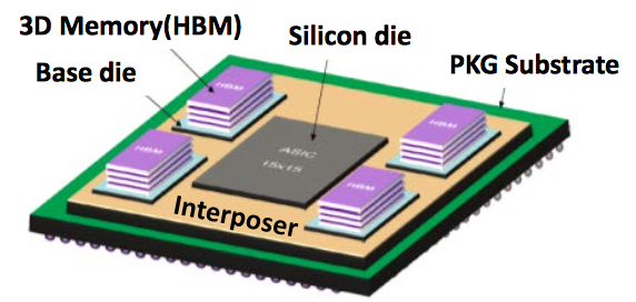
Rao brings his design experience to a substrate interconnect he calls an Interposer which streams data across a local network ( think of it as a hardware PTX )
The network IS the Interposer & its thread handling among HBM HybridMem queues, er.. streams .. whilst Async queues are a code driven watering hole .. (& of real benefit to data delays) it does harness the kernel somewhat slowing performance..less importantly teaching the serialization /DeSer programming model which is abstracted with Neon.
How this comes together without convenient kernel support libraries as found in CuSolver , is yet to be determined. Its main advantage lays in matrix manipulation , pattern recognition .. thus an object library of compiled IP functions makes sense for user defined data block size / k NN parameters / et al.
There is no available time to model Accelerated software except for an App , these days.. Look at OpenMP / OpenAccel a step in the right direction.. The learning curve (more than CUDA , what about failsafe, cluster database and server technology / display formatting) kills innovation in the product, word gets around & theres a copy of it on other hardware prior to release.. If Intel packs a function oriented prototyping toolbag , for a mobile Accel platform ( does this replace a phone GPU ?
At least my purchase of KU115 Kinetic/ Vivado Design is delayed until BSP for HBM is released by vendor, meaning 32GB on-board DDR4 is replaced by HCM. . the UltraRAM on the Ultra+ can be configured as a HybridCube.. only 360Mbits max available limits the thread per pattern issue for k-NN correlation (a very expensive function) Only very basic computes & certainly NEVER on a mobile platform.. I question the need to learn toolsets which target DataCenter OEMs if the App only needs to recognize smells (yes a sensor is avail) ..
https://www.xilinx.com/video/fpga/using-ultraram-in-ultrascale-plus.html
If cloud or not comes down to the same question: Trust level. Since ML and Deep Learning are all vulnerable to data input. If you feed it with corrupt data you can make the whole system basically garbage. So it is not only security against data breach & theft but also security about malicious data input, which is much harder and I doubt anybody of these DL shops have even thought about at all.
@OranjeeGeneral. I completely agree with that, but that is why we have the A.I. in place, plus verification modules. Data will always be corrupted somehow, someway. The important case in this math function it is for the C to be as small as possible F(x)+C.
Hope the baby isn’t thrown out with bathwater when it comes to AMD’s HSA, which purpose in part is too to shunt memory hierarchy. Less than 5x increase in throughput over current generation is not a good enough reason to spin custom silicon.
Well that’s 5 times raw you don’t know how much it is in terms of perW it might be a lot more than that. I could guess it is easily 10-20 or 40 times and then it definitely makes a lot sense. Also I think the second big selling points is the chipchip communication. A big bottleneck if you have large networks is going Multi-GPU for DL not that straightforward and scaling tethers off quickly too.
Nice to see the pioneering Transputer concepts rising to the surface again (you can’t keep a good architecture down!). Message-passing yes, no shared memory great, transparent and minimal-latency chip-to-chip communication even better.
It will be interesting to look into the underlying architecture to see whether it would also work for traditional FP applications.
Naveen Rao writes: “On our chip, which is a TSMC 28 nanometer chip, we’re seeing around 55 teraops per second.”
Just noticed GP102/104 (sm_61) + CUDA 8 make quad-rate int8 a primary target… hence that interesting number in current specs: 44 TOPS INT8. When Nvidia fold HBM into the mix (GV102 ?), will this affect those int8 TOPS?