
The end of Moore’s Law – the real Moore’s Law where transistors get cheaper and faster with every process shrink – is making chip makers crazy. And there are two different approaches to making more capacious but usually not faster compute engines – breaking devices into chiplets and linking them together or etching them on an entire silicon wafer – plus a third overlay that both approaches can employ with 2.5D and 3D stacking of chips to extend capacity and function.
No matter what, all of these approaches live under the tyranny of the reticle limit of the lithography equipment that is used to etch chips.
With current equipment that is tailored to 300 mm silicon wafers, that barrier is 858 mm2 and that is that. It is like the Terminator, or the speed of light in a vacuum. You cannot argue with it or bargain with it. No chip can be etched bigger than that. Moving from 150 mm wafers to 200 mm wafers to 300 mm wafers didn’t change that reticle limit over the past three decades, moving from visible light lithography to water immersion lithography to extreme ultraviolet lithography didn’t change the reticle limit. And the hypothetical move to 450 mm wafers would not have changed the reticle limit, either. Although we would point out that having 450 mm wafers would allowed more capacious waferscale compute engines here in 2023. But the engineering challenges for 450 mm wafers were too hard for IBM, Intel, Samsung, Taiwan Semiconductor Manufacturing Co, GlobalFoundries, and Nikon to solve, and that effort was abandoned in 2015.
The reticle limit – the size of the aperture that light passes through the chip masks to do the etching of transistors on silicon wafers – doesn’t just define how chiplets are designed, but it also limits the size of discrete blocks of compute and memory on a single wafer. It would be amazing if we had 450 mm wafers and all of the logic of a waferscale computer could be etched in one fell swoop with a reticle that was larger than the wafer, but that is not how lithography equipment works. When all is said and done, the difference between chiplets and waferscale is really about how one wants to construct the interconnects to make a compute engine socket out of discrete elements of compute and memory.
Despite this reticle limit, the industry always needs to build more capacious compute engines, and at the end of Moore’s Law, it would be nice if a way could be found if these devices could be cheaper to manufacture, too.
Researchers at the Institute of Computing Technology at the Chinese Academy of Sciences have just published a paper in a journal called Fundamental Research that talks about the limits of lithography and chiplets and proposes an architecture they call “Big Chip” that mimics the ill-fated waferscale efforts of Trilogy Systems back in the 1980s and the successful waferscale architecture of Cerebras Systems here in the 2020s. Elon Musk’s Tesla is creating its own “Dojo” supercomputer chip, but this is not a waferscale design but rather a complex packing of Dojo D1 cores into something that if you squint at it looks like a waferscale socket built from 360 chiplets. Perhaps with the Dojo2 chips, Tesla will switch to a true waferscale design. It doesn’t look like this would take a lot of work to accomplish such a feat.
The paper put together by the Chinese Academy of Sciences talks a lot about why one needs to develop waferscale devices, but it doesn’t provide much detail on what the Big Chip architecture they have developed actually looks like. And it does not indicate whether Big Chip will take the chiplet approach like Tesla did with Dojo or go all the way to waferscale like Cerebras did from the get-go. But the implication is clear that, just like Tesla, the Chinese government could fund such an effort if it wanted to.
According to the CAS researchers, the Big Chip implementation known as “Zhejiang,” which is Chinese for “crooked river and which is also the name of a mountainous, densely populated province in eastern China that has Hangzhou as it capital, will be done in a 22 nanometer process, presumably by Semiconductor Manufacturing International Corp (SMIC), the indigenous foundry in the Middle Kingdom that also has 14 nanometer processes ramped up and is working towards getting better yields with its 7 nanometer processes.
The Zhejiang Big Chip is comprised of 16 chiplets, each with 16 RISC-V cores. The researchers say that the design has the ability to scale up to 100 chiplets in a single discrete device, which we used to call a socket but that sounds more like a system board to us. It is not clear how those 100 chiplets would be configured or what kind of memory architecture would be implemented across those chiplets, which would have 1,600 cores in an array.
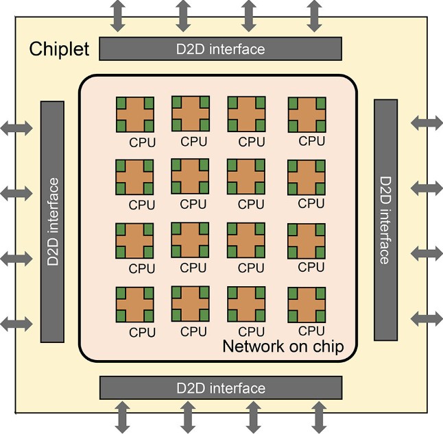
What we do know is that with the Zhejiang iteration of Big Chip there are 16 RISC-V processors connected to each other with symmetric multiprocessing across their shared main memory using a network on a chip, and there are SMP links between the chiplets so each tile can share memory across the entire complex.
Here is the block diagram for the Zhejiang RISC-V chiplets:
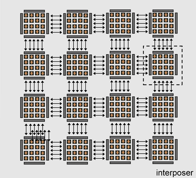
And here is how the die-to-die (D2D) interconnects are implemented using an interposer to lash 16 of these chiplets together into a 256-core compute complex with shared memory:
There is absolutely nothing that prevents this chiplet design from being implemented as waferscale, and the CAS researchers said as much. However, for this iteration, it looks like it will be chiplets using a 2.5D interposer interconnect, which is probably all that SMIC can muster at this point.
The interconnect is as important as the compute elements, as is always the case in system and subsystem design.
“The interface is designed using a channel-sharing technique based on a time-multiplexing mechanism,” the researchers write of the D2D interconnect. “This approach reduces the number of inter-chip signals, thereby minimizing the area overhead of I/O bumps and interposer wiring resources, which can significantly lower the complexity of substrate design. The chiplets are terminated at the top metal layer, where the micro I/O pads are built.”
While one Big Chip compute engine might be interesting as either a multi-chiplet or waferscale complex, what is important is how lots of these devices will be interconnected to provide exascale-class computing systems. Here is what the CAS researchers had to say about that:
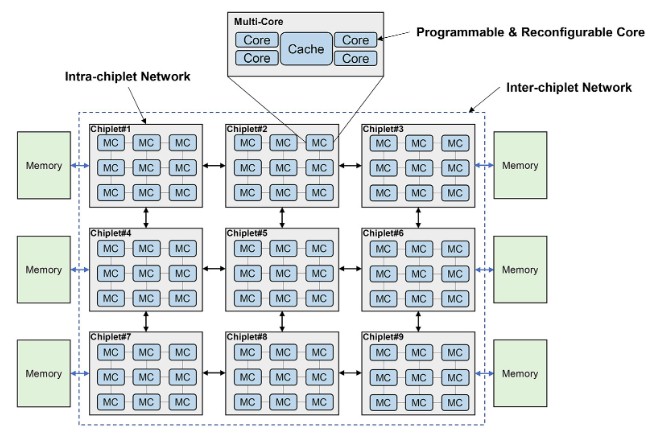
“For the current and future exa-scale computing, we predict a hierarchical chiplet architecture as a powerful and flexible solution,” the researchers write of this hierarchical structure of compute and memory, which is shown in the image below this lengthy quote from the CAS paper. “The hierarchical-chiplet architecture is designed as many cores and many chiplets with hierarchical interconnect. Inside the chiplet, cores are communicated using ultra-low-latency interconnect while inter-chiplet are interconnected with low latency beneficial from the advanced packaging technology, such that the on-chip(let) latency and the NUMA effect in such high-scalability system can be minimized. The memory hierarchy contains core memory, on-chip(let) memory and off-chip(let) memory. The memory from these three levels vary in terms of memory bandwidth, latency, power consumption and cost. In the overview of hierarchical-chiplet architecture, multiple cores are connected through cross switch and they share a cache. This forms a pod structure and the pod is interconnected through the intra-chiplet network. Multiple pods form a chiplet and the chiplet is interconnect through the inter-chiplet network and then connects to the off-chip(let) memory. Careful design is needed to make full use of such hierarchy. Reasonably utilizing the memory bandwidth to balance the workload of different computing hierarchy can significantly improve the chiplet system efficiency. Properly designing the communication network resource can ensure the chiplet collaboratively performing the shared-memory task.”
It is hard to argue with anything that is said in that quote, but the CAS researchers do not say how they will actually deal with these issues. And that is the hard part.
It is interesting that the cores in this diagram are called both “programmable” and “reconfigurable,” but we are not sure what that means. It might have to do more with a variable threading technique like IBM has with its Power8, Power9, and Power10 processors than with a mix of CPU and FPGA elements in the cores. It is hard to say.
The CAS researchers say that the Big Chip compute engine will consist of over 1 trillion transistors and occupy thousands of square millimeters of aggregate area, using either chiplet packaging or waferscale integration of compute and memory blocks. For exascale HPC and AI workloads, we think it is highly likely that CAS is thinking about HBM stacked DRAM or some other alternative double-pumped main memory like the MCR memory that Intel and SK Hynix have developed. It is possible that the RISV-V cores will have lots of SRAM local to compute, which might obviate the need for HBM memory and allow for the use of accelerated DDR5 memory using the MCR double-pumping techniques. A lot depends on the workloads and how sensitive they are to memory capacity and memory bandwidth.
The Big Chip paper has a wish list of prospective technologies, such as optical-electronic computing, near-memory computing, and 3D stacked cache and main memory that can be added to the Big Chip complex – and it looks like the use of optical I/O processors is at the top of the wish list. But CAS is not tipping its hand on what it is working on and when it might be delivered.
For all we know, Big Chip and its Big System are already built and CAS is just talking about it now. Google does things this way, for instance, but the time between rolling something into the field and talking about it has been shortening as companies like Google use interesting systems as a way to recruit techies.


Cerebras Shifts Architecture To Meet Massive AI/ML Models
What is that famous maxim in computer science about something that doubles on a regular cadence? Moore’s Law is one answer, but that’s a doubling (in this case, transistors) every two years. On a related note, we need a new term for machine learning models, which double in complexity every …

Mainstream Waferscale Closer Than It May Appear
The term “mainstream” in the context of the largest systems on the planet still only means a select few. But it is quite possible that proofs of concept for the sites building those huge future machines could set the stage for what’s next in some of the most demanding compute …
The Battle Begins For AI Inference Compute In The Datacenter
The major cloud builders and their hyperscaler brethren – in many cases, one company acts like both a cloud and a hyperscaler – have made their technology choices when it comes to deploying AI training platforms. They all use Nvidia datacenter GPUs and, if they have them, their own homegrown …
Have to read through thoroughly, but the Campus of the Lab is impressive. They just build the things.
“Xi – just do it!”, as it seems.
…well, it will also have its downsides, but yes, impressive and for sure attractive to academics.
Thanks Mr. Morgan for the article.
…forgot the links…
…its too late…should go to sleep…
https://en.zhejianglab.com/about/campus/Lab_Campus/
https://en.zhejianglab.com/OPPORTUNITY/lifeatZJLab/
Now you’re talkin’! This is what we want our international competitors to do (EU anyone?) — bring it on! Best way to beat the obesity epidemic (intellectually, after the holidays! Still recovering …). 8^p
You neglected to remind people that high-NA EUV halves the reticle limit.
https://spectrum.ieee.org/high-na-euv