
It has been two and a half decades since we have seen a rapidly expanding universe of a new kind of compute that rivals the current generative AI boom. Back then, with the Dot Com Boom, companies wrapped a layer of Internet networking and Web protocols around their prettified applications and made us all slaves to our mice and helped lay the foundations for the hyperscaler data miners that essentially run the Internet to this day.
Our mouse clicks get turned into their ad clicks. With the generative AI revolution, all of the text that we have ever created on the Web plus whatever else can be curated from private data sets and public domain books is scrubbed as clean of bias as can be done and a neural network is created linking trillions of snippets of words in this massive corpus with parameters that allow it to be a pretty effective question-answer system. Similar generative models have been made for images, video, and sound and corporations, governments, academia, and research institutions of the world are trying to figure out how to weave this into their applications, or how to create new ones, while also trying to figure out how they are going to get their hands on GPUs to train and run models as well as get the budget to pay for these massively parallel compute engines.
All throughout the machine learning AI revolution, which kicked off a decade ago but really accelerated with image processing at expert human accuracy in 2012, IBM has been working on its TrueNorth family of neuromorphic processors as well as complementary analog chips that can be used to AI inference and more traditional matrix math engines that are embedded in its Power and z processors and made available as discrete compute engines. But aside from the matrix units encoded in the Power10 and z16 processors, which are very different from each other, none of this has been widely or aggressively commercialized. Which is peculiar given the shortages of AI training and inference engines these days. You would think that IBM would show more hustle.
While we were on vacation back in late October, IBM’s research lab in Almaden, California – which works on AI and quantum computing as well as security and storage projects – announced the NorthPole kicker to the TrueNorth architecture, which was unveiled in Science as well as in a blog post by IBM Research. There was not a lot of technical detail made available to the public about NorthPole, which was a shame considering that it is the culmination of a life’s work for IBM Dharmendra Modha, an IBM Fellow and chief scientist for brain-inspired computing at the company.
The TrueNorth chips, of which we caught wind of way back in 2015 when IBM filed for patents on the design and which were more fully revealed in a paper in 2017 published by the IEEE, are like other neuromorphic chips in that they are literally physically inspired by the neurons in our brains and not just a neural network implemented in software with access to lots of vector and matrix math. Under the SyNAPSE program, IBM received $150 million in funding from the US Defense Research Projects Agency to create these neuromorphic chips, and due to the needs of the military, the TrueNorth and NorthPole chips focused on image and video recognition tasks.
The TrueNorth cores implements 256 neuron and 256 axons interlinked by a synaptic crossbar mesh, and then puts 4,096 of these cores – with memory local to each core – onto a single chip that was implemented in an unknown process (probably 22 nanometers but maybe fatter 32 nanometers) and that had 5.8 billion transistors emulating 268 million neurons. IBM networked 16 of these TrueNorth chips together as part of the DARPA project, and in 2018 a network of TrueNorth chips were used to do stereo vision processing.
NorthPole is an extension of the TrueNorth architecture, according to IBM, and this time around NorthPole has a clock like more conventional compute engines and unlike TrueNorth. In this case, it is a scalable clock, which runs at between 25 MHz and 425 MHz, depending on workloads, and is implemented in a 12 nanometer process. (That sounds like GlobalFoundries to us, but given the bad blood between IBM and GlobalFoundries over issues with the etching of two generations of Power and z chips, this seems difficult at best and unlikely at least.)
According to the Science paper, which you have to pay $30 to read and we did, the NorthPole chip has no centralized memory and instead distributes 224 MB of SRAM across the 256 cores in the chip. (That’s 768 KB per core.) It looks like NorthPole has much beefier cores, with each chip having only an array weighing in at 16 x 16 (for a total of 256 cores) rather than the 64 x 64 array of cores (for a total of 4,096 cores) used in TrueNorth.
As far as we can tell, the NorthPole cores implement straight up vector and matrix math instructions (in 8-bit, 4-bit, and 2-bit formats) and are not doing any emulation of synapses and axons in the cores or dendrites across the crossbar. Saying this is inspired by TrueNorth is a bit of a stretch; it looks more to us that it was inspired by Graphcore and SambaNova and Cerebras Systems. . . .
There are 22 billion transistors on the NorthPole die, which weighs in at a retical-stretching 800 mm2 area, and it can process 2,048 operations per core per cycle at 8 bit resolution, and obviously 4,096 operations per core per cycle at 4 bits and 8,192 operations per core per cycle at 2 bits.
There are two different networks on the NorthPole die, which IBM says are inspired by the long-distance white matter and short-distance gray matter networks in the human brain. (We did not know we had two different networks for cortical sensory and motor systems in our heads.) The short distance network on chip (NoC) allows spatial computing between adjacent cores and the long distance network allows neural network activations to be distributed across the cores.
The 16×16 array of NorthPole cores is front-ended by a set of sixteen frame buffers with a total of 32 MB of capacity, and these frame buffers (which look to be about the size of a NorthPole core) are in turn front-ended by I/O, queuing, and scheduling circuits. To process an image, it is chopped into sixteen pieces and fed into the 16 frame buffers.
Here is the rub, and what makes this neat: NorthPole is not a von Neuman architecture. And to quote the paper: “NorthPole exploits data-independent branching to support a fully pipelined, stall-free, deterministic control operation for high temporal utilization without any memory misses, which are a hallmark of the von Neumann architecture. Lack of memory misses eliminates the need for speculative, nondeterministic execution. Deterministic operation enables a set of eight threads for various compute, memory, and communication operations to be synchronized by construction and to operate at a high utilization.”
IBM says that on the ResNet-50 image recognition test and on the YOLOv4 object detection test, NorthPole is about 4,000X faster than TrueNorth.
Because data doesn’t move around so much in the NorthPole architecture, at least compared to von Neuman devices like CPUs and GPUs and their external main memories, IBM says NorthPole is more energy efficient per unit of work per unit of chip area, which are the metrics that chip designers are graded on and that hyperscalers grade on.
The Nvidia “Volta” V100 that was etched in a similar 12 nanometer process from TSMC has a comparable number of transistors at 21.1 billion and a comparable die size of 812 mm2, but the NorthPole device processes 25 times as many images per joule as the V100. And with the Nvidia “Hopper” H100 GPU etched in 4 nanometer TSMC processes and comprising 80 billion transistors, NorthPole delivers processes five times as many images per joule.
Here is how various compute engines stack up to NorthPole on ResNet-50 image recognition in terms of their frames/joule processing rate and their frames per second per billion transistors density:
![]()
IBM has been very clear that NorthPole is just a proof of concept. It has been tested running inference for the BERT encoder-only large language model from Google for natural language processing as well as on the Deep Speech 2 speech recognition model from Google’s DeepMind team. It has not been tested running inference on decoder-only LLMs like GPT-4 from OpenAI or LLaMA 2 from Meta Platforms, and Modha says IBM Research is looking into this.
We would say Big Blue should get a move on. Generative AI inference is way too expensive, and if NorthPole can be tweaked to support GenAI models, or the models can be tweaked to support NorthPole and scale across many devices, it is possible that IBM could get into the AI inference hardware game or at the very least provide AI inference side-cards with a lot more oomph than its on-chip matrix math units provide for the Power10 and z16 processors.
We do not think it is IBM’s goal to be a patent troll as it does such research and creates chips like TrueNorth and NorthPole. But we also do not think IBM takes itself seriously enough to spend the money to become an AI compute engine vendor in its own right and compete against GPUs and other ASICs for the tens of billions of dollars a year in AI systems that are going to be sold.
That could, of course, change. And should change, in fact. IBM just has to stop waxing its board and get into the water.

Ampere Arm Server CPUs To Get 512 Cores, AI Accelerator
With all of the hyperscalers and major cloud builders designing their own CPUs and AI accelerators, the heat is on those who sell compute engines to these companies. That includes Intel, AMD, and Nvidia, of course. And it also includes Arm server chip upstart Ampere Computing, which is taking them …
IBM Chips In To Drive 2 Nanometer Semiconductor Manufacturing
Big Blue got out of the chip foundry business when it sold off its IBM Microelectronics division to GlobalFoundries, itself a spinout of AMD, in 2014. The hope, no doubt, was that IBM could get out of investing in its foundries, which were not high volume facilities but expensive nonetheless, …
Arista Can Ride AI Up Past $10 Billion In 2026
In many ways, Arista Networks still behaves like a startup even though it was founded twenty years ago, rollout out its first products a little more than a decade and a half ago, went public a decade ago, and now as over 10,000 customers and over 100 million Ethernet ports …
Exactly! It’ll be interesting to see how this arch performs on decoder-oriented LLM processes and other GenAI which are the “hard” part of inference (eg. according to Cerebras’ Feldman in his HPCWire interview on the new Nvidia roadmap — that same roadmap which TNP pointfully questioned as well, and corrected!). A couple extra slightly “disheveled” Monday comments …
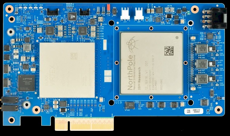
The two unknown-ish chips to the left of Northpole on the PCIe card (board photo) are, I believe, a Xilinx Virtex FPGA (silver-gray, large), and a Lattice FPGA (black, medium-size), likely used for I/O interfacing (markings somewhat visible by zooming and squinting!).
I wonder how broadly applicable “data-independent branching” (resulting in “deterministic control operation”) is, as a paradigm. It seems that parallelization is greatly eased where that independence arises (control flow graph only), but would exclude graph-traversal oriented processing (maybe CPUs are still best here? cf. Pingali et al., 2011. “The Tao of Parallelism in Algorithms”).
The multi-scale NoC is quite neat! (I might think of it as short-term and long-term memory loops … or not?).
The first sentence of the Conclusion to their Science paper is quite cool (IMHO) wrt perspective relativism: “As seen from the inside of the chip […] NorthPole appears as memory near compute; as seen from the outside of the chip […] it appears as an active memory.”. Wow!
Hmmmm … I smell a dish of recomposable disaggregated spaghetti monster calamari yumminess here! With trays of grilled CPUs linked to plates of “active memory” sauce, with plenty of CXL 3.0 optical fiber for throughput regularity! Think gastronomic cephalopods with an accurate deterministic left-brain that does math right, a lossy stochastic right-brain for tea and conversation, and a set of mesmerizingly luminescent pastafarian tentacles to bring it all together! A finest culinary of computational bliss! 8^b
I thought everyone knew “IBM” and “hurries” do not belong in the same sentence.
The “other chip” is a Xilinx Virtex FPGA, presumably hardware programmed for data streaming and PCI control. Although Northpole is ‘neuromorphic’, you will likely need a lot of the usual digital shuffling to get the ‘image’ cells filled, per core.
Thanks for clarifying. Appreciate it.