

Big Blue got out of the chip foundry business when it sold off its IBM Microelectronics division to GlobalFoundries, itself a spinout of AMD, in 2014. The hope, no doubt, was that IBM could get out of investing in its foundries, which were not high volume facilities but expensive nonetheless, and also create a stronger third party merchant foundry on which it could depend to manufacture its Power and z processors for the respective systems that it derives most of its revenues and profits from, one way or another.
That move, for which IBM actually paid GlobalFoundries $1.5 billion, would ironically also potentially help IBM’s CPU competitors in that it would create a stronger merchant player that could compete with Taiwan Semiconductor Manufacturing Corp, the world’s biggest and best chip foundry these days, which is a good thing. But the sale of Microelectronics also would also, in theory, help them make better CPUs that compete against Power and z processors, which is probably not a great thing but a fair trade given how customers using these platforms cannot easily move off of them.
Two funny things happened despite IBM getting out of the foundry business.
First, the company continued to do fundamental research in semiconductor technologies at its facilities in New York, usually in conjunction with AMD, Samsung, GlobalFoundries, and sometimes Intel. We don’t know for sure, but we suspect that IBM derives some revenues for this work, which in recent years has refined processes to bring 7 nanometer, 5 nanometer, and, as of today, 2 nanometer process technologies off the whiteboards and onto actual test chips. Perhaps IBM just sees this work as necessary to keep evolving its Power and z processors. It is unclear.
Second, GlobalFoundries pulled the plug on its 7 nanometer extreme ultraviolet (EUV) and regular water lithography efforts in August 2018, and therefore left IBM in a bit of a lurch until it could line up Samsung, which has huge foundries to make DRAM and flash memory but which is looking to ramp up a CPU foundry business for itself and for others, to be its foundry partner for the 7 nanometer technologies that are vital for the Power10 chip that is coming out this year. Power10 was originally slated to use a 10 nanometer technology from IBM itself or GlobalFoundries – it was never clear – but somewhere along the way it was bumped up to 7 nanometer etching and then the floor dropped out. But Samsung has rebuilt it, but the Power roadmap has been stretched out in time – just as Intel’s delays with its 10 nanometer and 7 nanometer processes have forced it to do a lot more tocking with architecture and a lot less ticking with process shrinks than it would like.
Looking ahead into the future five years from now has always been hard in the semiconductor business, but as Moore’s Law shrinkages in transistor sizes get more difficult and the expected proportional decrease in the cost of transistors flattens out, it has been particularly hard in recent years. That is why the breakthrough technology being announced by IBM Research today at its Albany, New York tech center, which shows a 2 nanometer CMOS process etching a real chip on a standard 300 millimeter silicon wafer, is so important. We are surprised IBM still does such research at all, and again, we presume this is a way for IBM to hedge its bets, make a little money, and help the foundry partners on which it depends. It doesn’t hurt to get good PR, either, but it is a little much when Big Blue talks about how it does “hard tech to differentiate hybrid cloud.”
This differentiation is clearly for sale. So it is debatable how differentiating it will bet when it finally comes to market and when IBM’s Power and z processors finally get to make use of it. But again, we are glad that IBM is doing this research and doing its part to help keep the process nodes coming. Big Blue has certainly done its share of research and development in the past, including creating single-cell DRAM several decades ago when the company still did its own memory chips, as well as creating chemically amplified photoresists and doing its own 3D chip stacking. IBM invented copper interconnect wiring in 1997, replacing aluminum wires on semiconductors, radically improving performance and cutting power consumption for transistors. IBM also invented silicon-on insulator techniques in 2000 and low-k dielectrics in 2001, and all of these technologies were brought to bear in the Power4 processor launched in 2001 that made it such a beast compared to its RISC and CISC rivals. These technologies allowed Big Blue to do multicore CPUs and eventually embedded DRAM for its L3 caches on the Power and z chips. High-k/metal gate technologies, which debuted in 2008, also helped Power and z CPUs push the architectural envelope.
This much is clear: Chip manufacturing technologies enable chip architecture leaps. So perhaps it is just obvious why Big Blue wants to chip in and do its part. It is enlightened self-interest at work, and may cost as much or more than the money it generates.
Three Nanosheets To The 2 Nanometer Wind
Mukesh Khare, who is currently vice president of hybrid cloud research at IBM, walked us through the 2 nanometer breakthrough. (That title seems utterly silly if Khare is really working on semiconductor research.) Khare worked on the 90 nanometer SOI process from 1999 through 2003, the one that brought Power4 and Power4+ to market, and managed the 65 nanometer and 45 nanometer SOI follow-ons that were used with Power5 and Power6 processors; he then did research on the 32 nanometer technology used for Power7 and then worked on high-k/metal gate technology used in the 22 nanometer processes that were employed on Power8. Khare then went on to be director of semiconductor research at the Albany NanoTech Center, and then took a stint as vice president of IBM’s Systems technology before being given the vice president of hybrid cloud research gig last July.
Here’s the gist of the 2 nanometer chip manufacturing techniques that IBM has cooked up:
There is a bunch of stuff in there, so let’s unpack it a little.
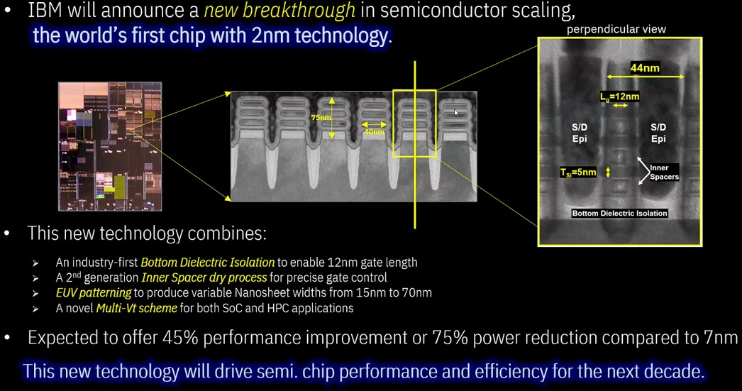
First, this is called a nanosheet stacked transistor, and it stacks an NMOS transistor on top of a PMOS transistor instead of having them sit side by side to take voltage signals and flip bits from one to zero or zero to one. These are also sometimes called gate all around, or GAA, transistors, and they are the next evolution in 3D transistors from FinFET technologies used for the past several generations of transistors from TSMC, Intel, GlobalFoundries, and others. FinFET transistors pulled the source and the drain channels for the transistor up into the gate, and nanosheets embedded multiple source and drain channels into a single gate to jack up density. IBM says that the test chip it has created with its 2 nanometer processes can allow 50 billion transistors in a chip the size of a fingernail. This is not the kind of precision – or lack thereof – that we here at The Next Platform like. But we give you the data as we can get it.
In this case, there are three layers to the nanosheet, and each sheet has a width of 40 nanometers and a height of five nanometers. (There is no feature that is measured that is actually at 2 nanometers. These terms are largely descriptive, not literal, which is maddening. Think of it as what the gate sizes would have to be if they were still planar, which they are not. I think. Maybe.) If you look on the right of the chart above, that is a slice of the nanosheet showing the side view, which has a pitch of 44 nanometers and a gate length of 12 nanometers, which Khare said would be the sizes used by most 2 nanometer processes in the remaining foundries that will do this.
The 2 nanometer chip manufacturing also includes the first use of what is called bottom dielectric isolation, which curtails current leakage and therefore helps to reduce the power consumption on the chip. That’s the light gray bar that is sitting underneath the three stacked transistor sheets in the middle cross section in the chart above.
Another new technique IBM has created for the 2 nanometer process is called the inner space dry process, which on the face of it sounds uncomfortable but which actually allows IBM to have precise gate control.
The experimental process also includes more widespread use of EUV technologies, and includes EUV patterning on the front end of the chip process, not just in the middle and at the back end, where EUV is being used with 7 nanometer processes today, and importantly, all critical features will be etched with EUV lithography and IBM has also figured out how to use single exposure EUV to reduce the number of optical masks used to etch chips. The net effect is that it will take many fewer steps to create a 2 nanometer chip than it does for a 7 nanometer chip, which should boost the throughout of fabs and perhaps reduce the cost of a finished wafer some, too. (We shall see.)
Finally, the 2 nanometer transistors have a threshold voltage (Vt in the chart above) that can be scaled up and down as needed, say a lower voltage for handheld devices and a higher one for CPUs used in exascale supercomputers.
IBM is not saying whether or not this 2 nanometer technique will employ silicon germanium channels, but there is a possibility, apparently.
This 2 nanometer process is expected to offer transistors that can run 45 percent faster or run at the same speed and reduce power by 75 percent compared to the current 7 nanometer process that will be used with the Power10 chip and is analogous to the 7 nanometer processes from TSMC and in some ways to the 10 nanometer and 7 nanometer processes from Intel.
Now, we know what you are thinking. First, will Power11 chips use this 2 nanometer process? And second, what on earth comes after this? A 1 nanometer process seems pretty impossible, doesn’t it?
Let’s talk Power roadmaps for a second. Power10 is in 7 nanometers and given the conservative and legacy nature of the Power and z server businesses, which are on a three year cadence for processor updates, Power11, which is already under design, and Power12, which is being whiteboarded, do not have to just rush off to 2 nanometer when there are 5 nanometer and 3 nanometer nodes to use before getting to the 2 nanometer node, which Khare expected to be ready for production by the end of 2024. Power11 should be expected sometime around 2023, and it should be on a mature 5 nanometer process, which means it will be relatively cheap. (Cheaper than being on 4 nanometer, or 3 nanometer, or 2 nanometer processes, which is the relative part.) IBM is probably not going to be in any hurry to rush off to 2 nanometers because after that, the move is to nanowires and who knows how that is going to pan out.
It seems far more likely that IBM will move to chiplets with Power11 in 2023 or 2024. We say 2023 if you want to get back to the original three year cadence because Power10 was originally supposed to be in 2020 on a 10 nanometer process (sound familiar, this delay?), and that means Power11 should be in 2023. That’s a year ahead of the 2 nanometer process going into production, probably at Samsung and Intel. By the way, Intel has just partnered with IBM for its Intel Foundry Services and has its own nanosheet approaches. Khare did not confirm that Intel would be using this IBM tech, but it ain’t hard to see that it will have access to it. And who knows? Intel could end up being IBM’s foundry partner is Samsung messes something up. That probably means that Power12 in about 2026 will be on the 2 nanometer process, and that gets to product line to 2029 or maybe 2030 before hitting the Moore’s Law wall.
Which brings us to the obvious question: What on Earth do you do after 2 nanometers, and are we going to hit a wall?
“I don’t think there is a wall that we can’t break through, and I would say there are many more breakthroughs that are coming in the pipeline and we will be sharing more and more as technology matures,” says Khare, with a nice turn of phrase. “I don’t see a wall, I see a lot of opportunities and a lot of things that we can innovate to keep going.”
Don’t you love the smell of optimism?

IBM Starts Walking The Hybrid Cloud And AI Talking
If Big Blue is going to talk the hybrid cloud and AI talk, as it seems to do incessantly, then the company has to walk it. And perhaps the most interesting thing that was said as part of the company’s discussion of its first quarter 2023 financial results was its …
Enterprises Are Not Going To Miss The Fourth Wave Of AI
IBM announced its Watsonx software development stack back in May, and today it is starting to ship it to customers. We wanted to know exactly what the heck it is. And so we reached out to Sriram Raghavan, vice president of AI strategy and roadmaps at IBM Research, to get …
Big Iron Will Always Drive Big Spending
Starting way back in the late 1980s, when Sun Microsystems was on the rise in the datacenter and Hewlett Packard was its main rival in Unix-based systems, market forces compelled IBM to finally and forcefully field its own open systems machines to combat Sun, HP, and others behind the Unix …
>>it stacks an NMOS transistor on top of a PMOS transistor instead of having them sit side by side
Can you highlight where this was said? I didn’t notice this claim from IBM. The photomicrograph seems to show a ‘traditional’ nanosheet transistor structure, with each of the three channels in the stack having the same gate.
As an historical aside, during the planar-transistor era the dimension in the node name described the channel length. IBM is coming clean here by acknowledging that its 2nM process implements 12nM channel length, hence a mere factor of six spec bloat.