

The great thing about the Cambrian explosion in compute that has been forced by the end of Dennard scaling of clock frequencies and Moore’s Law lowering in the cost of transistors is not only that we are getting an increasing diversity of highly tuned compute engines and broadening SKU stacks across those engines, but also that we are getting many different interpretations of the CPU, GPU, DPU, and FPGA themes. There is enough commonality across these device families that some modicum of compatibility is possible, but one could argue that cloning and copying devices is not only not necessary, but undesirable.
And that means the chances for the co-design of harware and software are increasing just as we need it most. Our very different software horses are getting very different hardware courses in which to run.
It is into this ever-diversifying compute world that AMD is putting out the best CPUs and GPUs it has ever designed for the datacenter, and is also bringing to bear the FPGAs and DPUs that it got through its acquisitions of Xilinx and Pensando. And the competition that AMD is compelling is creating a positive feedback loop of innovation in the adjacent Arm and RISC-V CPU markets and accelerators based on the RISC-V architecture.
We think, in fact, that the pace of innovation in the Instinct GPUs in particular is happening even faster than AMD and its initial customers had anticipated. For instance, we are fairly certain that Lawrence Livermore National Laboratory, which is the flagship customer for the APU variant of the MI300 series GPUs known as the MI300A, fully expected to have a server node in its “El Capitan” system that was based on the same fundamental architecture as the “Frontier” supercomputer – one AMD Epyc CPU with four Instinct GPUs attached to it coherently with Infinity Fabric links so the CPU and GPUs could all share their memories.
We know this because way back when, in March 2020 when AMD was awarded the CPU and GPU parts of the El Capitan system, Lawrence Livermore said this, and was in fact emphatic that unlike the Frontier system, which had a custom “Trento” Epyc CPU and a semicustom MI250X GPU (both upgraded to have coherency across Infinity Fabric), El Capitan would use off-the-shelf, discrete Epyc CPU and Instinct GPU components from AMD.
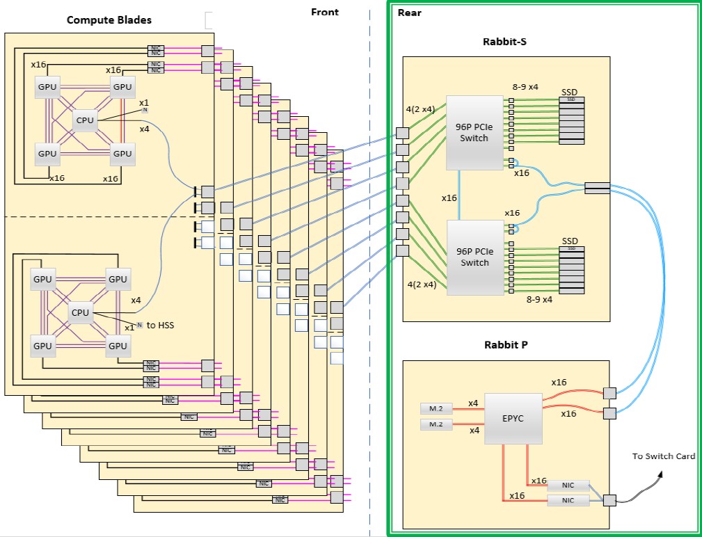
Like this, which shows the El Capitan compute nodes in a 1×4 configuration linked to the “Rabbit” distributed storage:
And yet, in the form it is being delivered later this year, El Capitan does not use standard AMD parts. Somewhere between then and now, a better deal came along because AMD got even better at making chiplets and integrating them in innovative – and affordable – ways. This deal, to be specific, looked like this:
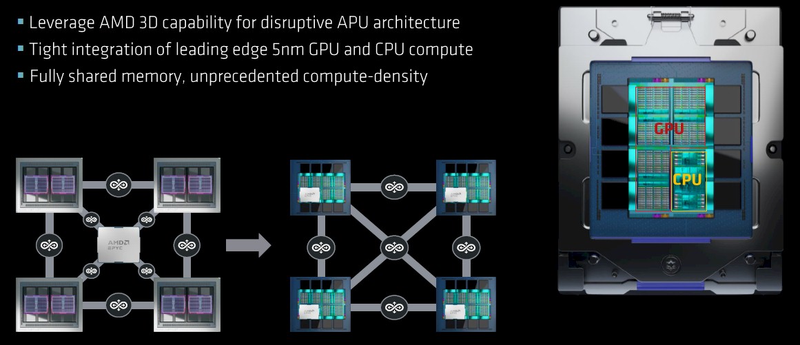
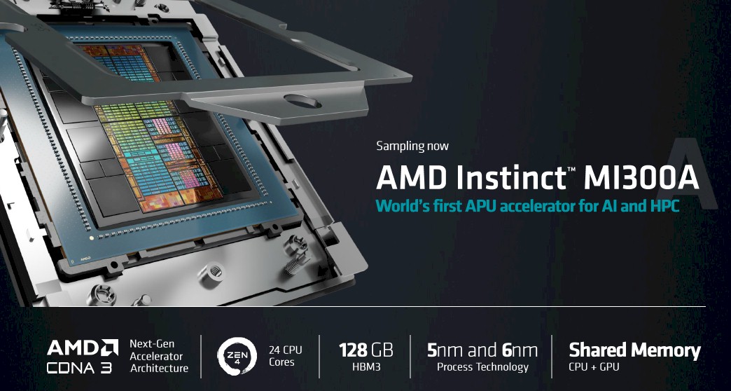
The creation of the MI300A Accelerated Processing Unit for datacenter compute, by which AMD means a system on chip that includes both CPU and GPU processing with coherent shared memory across them, is the culmination of work that started out way back in 2006 with something called Project Fusion, which has resulted in some interesting desktop and laptop hybrids but not a true APU for the datacenter. The first datacenter APU to market, from AMD or anyone else unless you want to call an Nvidia “Grace” CPU and “Hopper” GPU hybrid an SoC instead of two tightly coupled discrete devices with their own memories – is with the El Capitan system. And as we long suspected, there is the MI300A APU variant of the MI300 series as well as a discrete, standalone GPU version, which we now know is called the MI300X thanks to its unveiling today at the company’s Data Center & AI Technology Premiere event in San Francisco.
Clearly, reducing the latency between the CPU and the GPU and having fully shared identical memory as opposed to fully coherent discrete memory on each device was very appealing to Lawrence Livermore. And so, somewhere along the way, AMD’s APU dreams met Lawrence Livermore’s needs and we have the MI300A.
But having fixed ratios of CPU and GPU compute on a single device is not necessarily the best way to address the diverse needs of the market, as Intel has recently argued when it comes to AI training workloads in particular as it killed off its own XPU (Intel would rather die than use an AMD abbreviation for a technology) hybrid CPU-GPU datacenter compute device, previously and still known as “Falcon Shores,” but this time instead of being an XPU, Falcon Shores, due in 2025, is a GPU that will make use of the matrix math engines and Ethernet fabric interconnect of the “Gaudi” line of neural network processors, which will be discontinued after the Gaudi3 device comes to market sometime around the third quarter of next year.
Whatever codename AMD is using for its third generation of Instinct GPUs, we don’t know it and no one else does, either. So we have codenamed it “Antares,” which is consistent with the star codenames that AMD used for the first and second generations, “Arcturus” and “Aldebaran” to be specific. All are bright stars in the sky that begin with A. Why not? We need synonyms.
Here is the reveal on the Instinct MI300A:
There is not much new here except that there is not a deliberate obfuscation of the CPU cores as happened back in January this year:
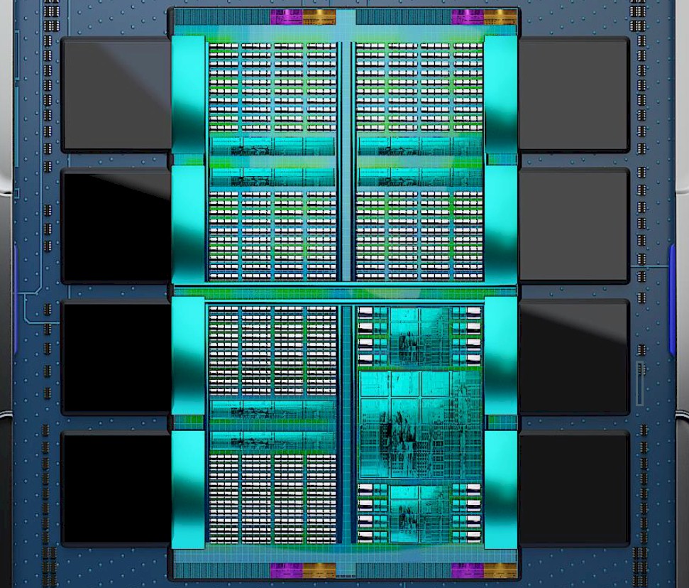
Which sent us down a weird rathole thinking there was an I/O die in the center of two 16-core Genoa chiplets with a quarter of their cores inactive. The new die shot above, which we zoom in one below, clearly shows three 8-core Genoa chiplets:
So that ends that mystery.
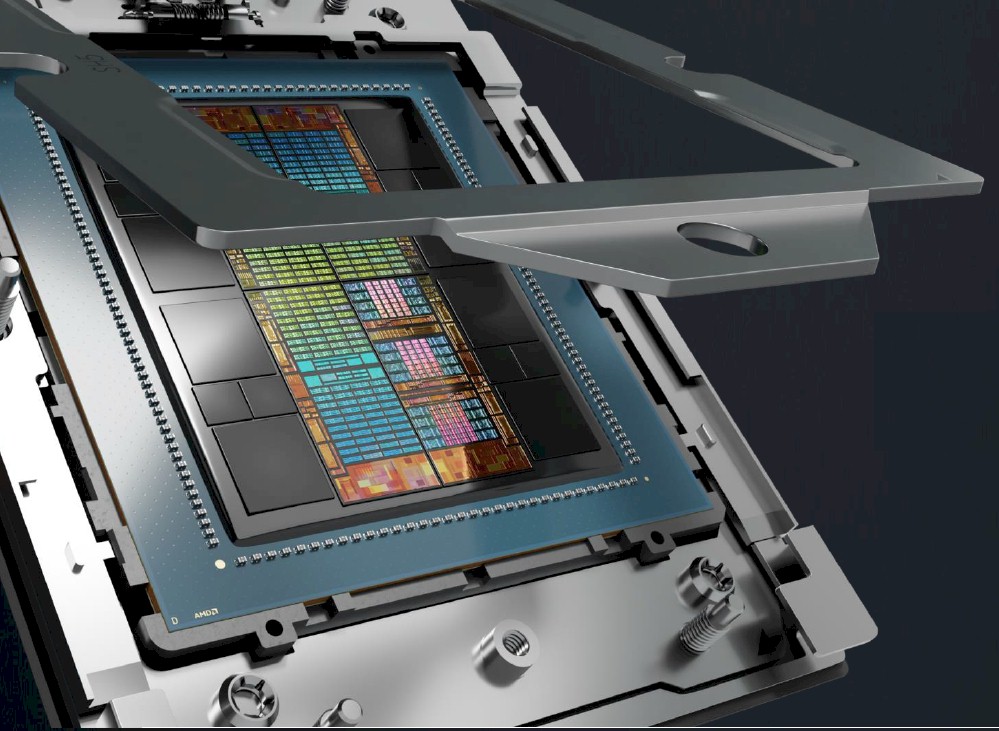
Here is the reveal on the MI300X GPU accelerator, which is a discrete device that is completely comprised of GPU chiplets for compute:
To make the MI300X, you pop off the three Genoa eight-core chiplets and you plunk down eight Antares GPU chiplets to fill out the socket. The two MI300 packages have eight HBM3 stacks at 32 GB each (eight high at 4 GB a pop is our guess), which means the devices can in theory max out at 256 GB of HBM3 memory. It looks like six of the eight stacks, for a total of 192 GB of capacity, are active on the MI300X, while only four of the eight stacks, for a total of 128 GB of capacity, are active on the MI300A. It could be that the MI300A has eight four-high stacks for half capacity for full bandwidth at a certain thermal point. So Lawrence Livermore is perhaps sacrificing some GPU compute capacity on a converged device as well as HBM3 memory capacity to integrate those Genoa cores directly on the MI300A GPU accelerator, but maybe getting full bandwidth. We shall see.
Here is our update on the feeds and speeds of the MI300A and MI300X, which we first presented a few weeks ago when talking about sky-high GPU accelerator prices and which has been updated with new estimates as well as a few tidbits of new data from AMD:
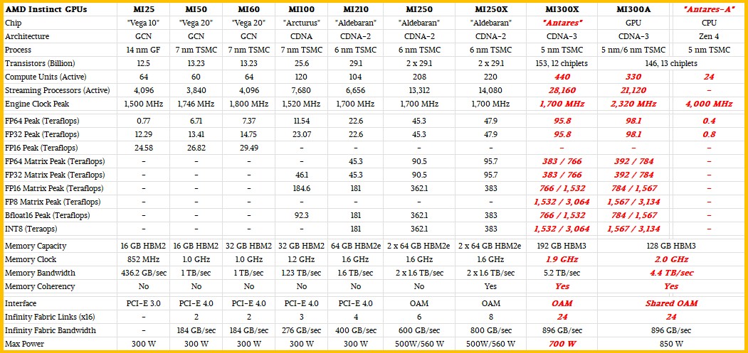
Some explanations of how we think the MI300X and MI300A will play out. We know that the MI300A is hot, at 850 watts. So we think Lawrence Livermore was only willing to give up two GPU tiles on an MI300 device if it could get it to clock faster. That’s what we would do if we were building a supercomputer. Our model says push it a little further and drive performance above the MI300X, in fact. Fewer memory stacks means lower bandwidth, and that will affect workload performance. Maybe the clock speed will be lower on the MI300A or the same as the MI300X. All we are saying is this is what we would try to do, and maybe this is what Lawrence Livermore did the same. It’s a thought experiment, not inside information.
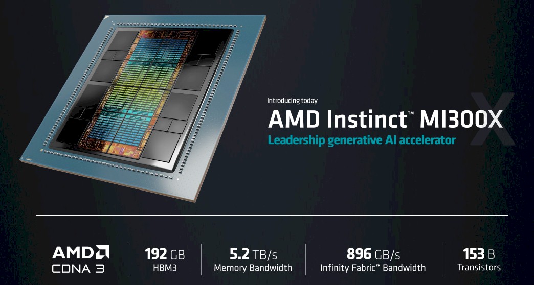
The MI300X has 153 billion transistors across 12 chiplets, and is, as AMD chairman and chief executive officer Lisa Su explained, the most complex compute engine that AMD has ever created. With its 192 GB of main memory, it can hold up to 80 billion parameters at FP16 half-precision floating point, she said, and therefore can hold an entire large language model of that size or smaller for AI inference within a single GPU. The gap, says Su, compared to the competition – Nvidia “Hopper” H100 GPUs presumably not including their “Grace” memory extenders and CPU auxiliary processing – looks like this for AI inference for various models:
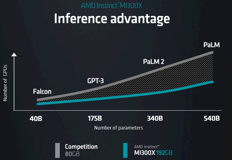
We would add that equally importantly, because the device has so much memory, in scale-up and scale-out clusters of GPUs, it also means it takes fewer GPUs to amass the memory to train those large language models, too.
The Instinct MI300A has 146 billion transistors across its 13 chiplets, and that transistor count was given out back in January but we were not sure if it was for the CPU-GPU hybrid or the GPU-only device when AMD said it. Now we know.
One last thing. AMD has cooked up a little something called the AMD Instinct Platform, which puts eight of the MI300X GPUs and 1.5 TB of HBM3 memory into an industry standard, Open Compute-compliant, Universal Base Board (UBB) form factor. Intel has done the same for its “Ponte Vecchio” GPUs, which also plug into Open Compute Accelerator Module (OAM) sockets. Both Microsoft and Facebook put forth the OAM and UBB standards, and they absolutely want GPUs that adhere to these if they can get them, and if not, they want Nvidia HGX boards with their SXM4 and SXM5 sockets to at least fit in the same enclosures without modification.
The MI300A is sampling now and will be shipping later this year, presumably in time for El Capitan to make it onto the November 2023 Top500 rankings as the most powerful supercomputer in the world. The MI300X will start sampling in the third quarter and is expected to start shipping by the end of the year. The launch of the MI300 family of GPU accelerators, complete with feeds, speeds, and hopefully pricing, is slated for later this year – our guess is around the SC23 supercomputing conference in November, perhaps the week before.
Heaven only knows what they might cost. If you have to ask you can’t afford it. . . . But probably in the neighborhood of $20,000 with supply shortages pushing up street prices to perhaps as high as $30,000.


“Which sent us down a weird rathole thinking there was an I/O die in the center of two 16-core Genoa chiplets with a quarter of their cores inactive. The new die shot above, which we zoom in one below, clearly shows three 8-core Genoa chiplets:”
is that the New Die shot Below and the Old one Above and maybe label each respective Image as Old Versus New to avoid any confusion that sometimes comes with wording only!
Good point. It was very late in the evening.
Hello Timothy,
You write “The MI300X has 153 billion transistors across 12 chiplets, and is, as AMD chairman and chief executive officer Lisa Su explained, the most complex compute engine that AMD has ever created.”
However, 192GByte of HBM3 is (assuming 1T per bit/cell) = 192G x 8 = 1.536 trillion transistors, I think, for the memory alone.
Great info, thank you!
True enough, but no one is counting the main memory transistors in any of these comparisons. L4 cache down to L1 cache, down to registers and TLBs, sure. It is funny to think about though, isn’t it? The compute transistor budget is this complex spec in a vast sea of memory monotony.
Grace Hopper BTW, has 80 billion transistors for comparison (to 148 billion).
AMD have a big GPU scaling advantage, by at long last applying chiplet tech to GPUs.
Nvidia’s monolithic GPUs ~cannot scale further.
Why is the MI300A lower precision estimates higher than your MI300X estimates?
A vestigial mistake from an earlier model I didn’t catch. The FP64 and FP32 are too low for this scenario. Fixed. And thanks.
Cool, thanks. But I don’t see a change/update yet in the chart. Is the result skewed partly due to the frequency you have the CUs running at? Thanks!
Yes. I am suggesting that the HPC flagship will overclock. The FP64 and FP32 vector were assuming virtual the same clock, which was my original assumption. Then I saw the official 850 watt rating and thought, maybe they are overclocking it….
The “Inference advantage” slide compares “number of GPUs” on the vertical axis. The blue line in the chart appears have under-counted by multiples of 8 for some odd reason.
My favorite bit of the ingenuity of AMD is they have put the IO die into a base die with the infinity cache as a L3 cache below the GPU and CPU chiplets.
I am looking forward to seeing how this all works. It would make one hell of a CPU with all Genoa cores….
Somebody must be interested in the all CPU version for them to have that sku…
I’ll take one.
Is it just me or i think the memory configurations is either 16GB x 8 for the MI300A & 24GB x 8 for the MI300X, That’s why the X is sampling later compared to the A because 24GB HBM3 stack also came at a later date than the 16GB stack as per SK Hynix announcement (in which i believe the module is provided by them)