
Disaggregation means a lot of things, but the one thing that it most certainly does not mean is that every little thing in a system necessarily has to be smashed apart and then put back together in a composable ways. Sometimes, it makes sense to aggregate devices in new and more useful ways physically even as you disaggregate those very same components logically.
That, in a nutshell, is what compute and storage fabric maker Enfabrica, which is dropping out of stealth mode at the MemCon Conference being hosting this week in Silicon Valley, is proposing is the best path to tackle the architectural challenges as more and more high performance workloads – traditional HPC simulation and modeling, AI training and sometimes large-scale inference, and various kinds of advanced data analytics – have a mix of compute and memory that go beyond a CPU and its memory in a chassis and that often span dozens to hundreds to thousands of nodes.
We spoke to Enfabrica back in June 2021, a little more than a year after Rochan Sankar, its chief executive officer, and Shrijeet Mukherjee, its chief development officer, started the company, and we profiled them in detail at the time – and if you didn’t read that story you should because the context is important if you really want to understand the Accelerated Compute Fabric, or ACF, silicon that Enfabrica has created.
It is also warranted to remind you that Mukherjee did high end graphics systems at Silicon Graphics, was director of engineering for the “California” Unified Computing System server-networking hybrids at Cisco Systems, ran software engineering at open source networking software provider Cumulus Networks, and did two years at Google working on network architecture and platforms before joining Sankar to establish Enfabrica. Sankar was an application engineer and chip architect at Cypress Semiconductor and is familiar to readers of The Next Platform as the director of product marketing and management at Broadcom, driving five generations of its “Trident” and “Tomahawk” datacenter switch ASICs, which sold over 300 million ports during his tenure.
Enfabrica has a bunch of other heavy hitters who have thought over the compute, storage, and networking issues that are confronting the modern datacenter, and it is important to point some of them out before we dive into what Enfabrica is actually going to do. The company’s founding advisor is Christos Kozyrakis, a professor of electrical engineering and computer science at Stanford University and the director of the Multiscale Architecture and Systems Team (MAST) who has done research stints at Google and Intel, among other organizations; he has done extensive work on vector processors, operating systems, cluster managers for clouds, and transactional memory systems. Another heavy hitting advisor is Albert Greenberg, who is currently vice president of platform engineering at Uber, who was in charge of Azure Networking at Microsoft for more than a decade after being a researcher at the software giant for four years, and who was a network guru for AT&T Bell Labs before that. Rachit Agarwal, an associate professor at Cornell University who has expertise in large-scale data analytics, is also an advisor.
The direct Enfabrica team includes Mike Jorda, who was director of integrated circuit design at Broadcom for more than two decades, and who now has the same job now at Enfabrica. Michael Goldflam, who did a decade and a half at Broadcom as director of its switching software, is in charge of systems testing at the startup. Carlo Contavalli, which was “Supreme Packet Juggler” at Google for more than a dozen years, is in charge of software engineering, and Thomas Norrie, a hardware engineer who was at Google for the same time and who was instrumental in the development of that hyperscaler’s homegrown SSD and TPU AI accelerators, is principal architect at Enfabrica. Gavin Starks, who was chief technology officer at SmartNIC maker Netronome Systems, is silicon architect for the company.
As far as we can tell from poking around the Internet, Enfabrica has around 85 employees and has raised $50 million in early stage venture funding from Sutter Hill Ventures. Stefan Dyckerhoff, managing director at the company, was a ASIC designer at Juniper Networks, did a stint as manager of routing products at Cisco, came back to run switching at routing at Juniper, and joined Sutter a decade ago as part of the investment in Skyport Systems, which was acquired by Cisco to bolster its security products.
Suffice it to say, this team not only knows the datacenter, but it knows how to bring products to market.
The Magic Bullet
No one outside of Enfabrica really knew what it was up to a year ago because the company was understandably secretive. But with its silicon shipping sometime this year, and the first quarter of this year nearly gone, the MemCon 2023 conference is a good place to start and this is a good time to do it.
Enfabrica is not trying to hit many targets with many bullets but is targeting many of the bottlenecks across the datacenter with one bullet, which it calls the Accelerated Compute Fabric Switch, or ACF-S for short.
This disaggregated and composable fabric approach reminds us a bit of TopSpin, which emerged using the InfiniBand fabric during the Dot-Com Boom and which was bought by Cisco in April 2005 for $250 million and never properly productized and promoted. Everyone at Enfabrica knows this, and is intent on not making the same mistakes that TopSpin and Cisco did way back then.
Anyway, the target is everything juicy and interesting in the datacenter that has to do with storing, processing, and moving data around at scale, says Sankar, throwing out this chart, which is based on forecasts from Gartner, IDC, and 650 Group.
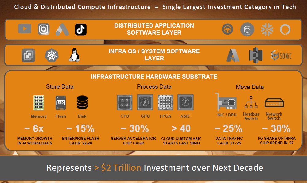
With the networks share of the semiconductor pie getting larger and larger (as it did during the 40 Gb/sec and early 100 Gb/sec days before PAM-4 signaling was perfected in network switching) and for overall I/O semiconductor spending to comprise a whopping 30 percent or so of all chip spending in the datacenter by 2027, something has got to give. In fact, the way Enfabrica sees it, a whole lot of things are going to have to give to get this $2 trillion total addressable market in the datacenter over the next decade under control.
“With the ChatGPT large language model going from zero to 100 million users in a month, it has put a highlight on the dimensions of scaling and how that changes the relationship between compute and memory, or between CPU and GPU compute,” Sankar tells The Next Platform. “As for what is the right datacenter architecture going forward, I think people are running so fast that their TCO models have not yet caught up to exactly how brutal it could look if all things scaled. It could get very expensive. What is clear to us is that there is a step function needed in bandwidth per dollar and that we need to unleash stranded resources through a new kind of bin packing. We are building a much more elastic, aggregated unit of bandwidth to collapse the tiers of PCI-Express, RDMA switching, network interfaces, and rack-scale interconnect.”
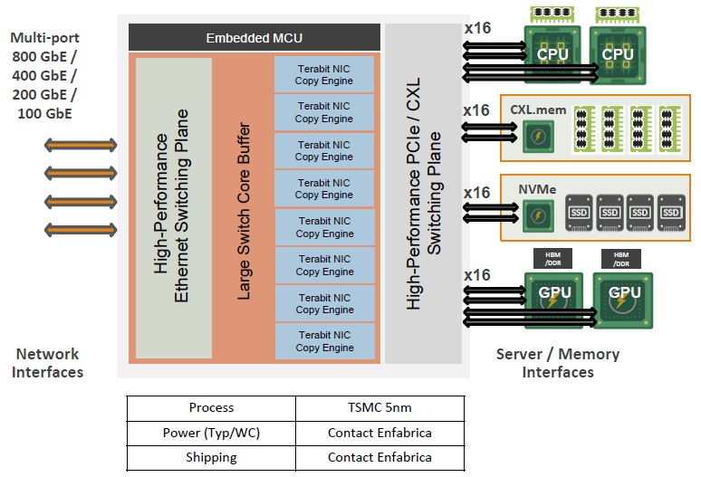
Here is what the Accelerated Compute Fabric – which we will point out also has both memory and persistent storage so the name is not perfectly suited to convey the idea behind the technology – looks like:
The advent of the ACF chip by Enfabrica goes against the increasingly prevailing wisdom of putting intelligence in the switch itself, inside of network interface cards (which have had various kinds of acceleration for years), and even to goes so far as to do away with the need for things like DPUs or IPUs, whatever you want to call them.
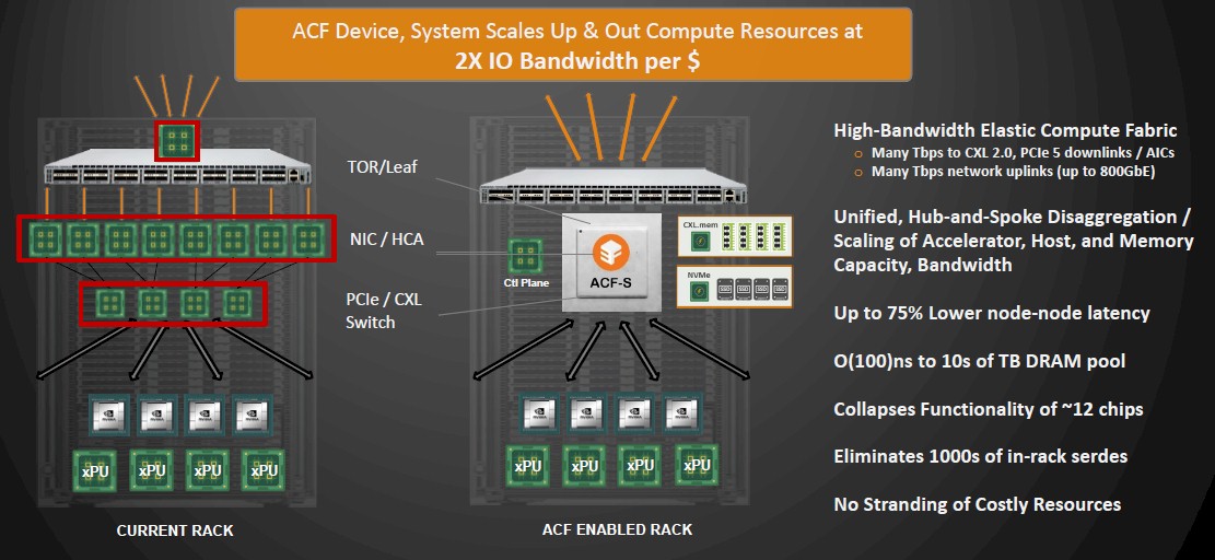
The ACF does this by being a kind of hybrid device that brings together an Ethernet switching plane that scales up to 800 GB/sec with a PCI-Express/CXL switching plane for peripherals, with NIC copy engines and a large switch core buffer in between the two. The precise bandwidth, port counts, PCI/CXL lanes, and such are not being divulged, but Mukherjee says that the first device will deliver a “multi-terabit server fabric.”
The ACF chip, in fact says Mukherjee, collapses down the functionality of around a dozen chips and eliminates thousands of SerDes in a typical server rack while providing up to 75 percent lower latency and an interconnect that can provide CXL 3.0-like functionality today, allowing tens of terabytes of memory to be pooled that is a few hundred nanoseconds away from compute in the span of a few racks.
These ACFs can be hooked together in a hub and spoke fashion to scale, and Enfabrica says that it can scale to many thousands of nodes in an AI cluster crammed with GPUs or other kinds of accelerators compared to the hundreds of devices using PCI-Express switching or clusters based on InfiniBand as is commonly used to lash GPU-heavy nodes to each other. The use of the ACF hybrid network devices means that a GPU-heavy rack aimed at AI training workloads can cut its power by at least 10 percent compared to current cluster designs, and the TCO of the ACF approach is up to 40 percent lower than the way AI systems are architected today with a combination of NVLink in the node and InfiniBand across the nodes. Because GPU utilization is driven higher by the lower latency networking, training times are faster for a given set of GPUs.
“Think of this as sort of a hybrid between a NUMA network and a classic Ethernet switch fabric,” Mukherjee tells The Next Platform. “It has guaranteed operations within its domain, and it is not just highly predictable, it is completely predictable. There’s no statistically multiplexing, there’s no reduce to Clos and then see if it works out. But the difference is on the left side, it looks like a packet and once it goes into the Ethernet world, all bets are off. We can help. We can steer, we can spray, we can do all kinds of interesting things, but all bets are off. If it stays on the right hand side, then it’s guaranteed delivery because of PCI semantics.”
What we thought was interesting was the prospect of just networking trays of GPUs to ACFs with very few CPUs at all. You could, in theory, have one host machine that sees all of the GPUs as a giant NUMA-like – and in a way NVLink like – GPU cluster. Sankar and Mukherjee just laughed when we said this, and Mukherjee said that the number one issue that every GPU team wrestles with is how many CPUs to put into the pipeline. Maybe the answer is, in fact, none.
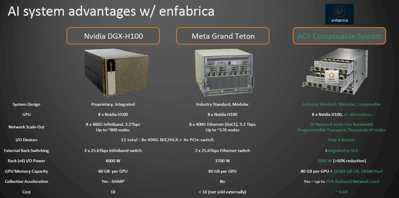
Here is how Enfabrica compares a composable system based on the ACF chip to the DGX-H100 system from Nvidia and the “Grand Teton” AI server from Meta Platforms:
We look forward to seeing how system makers deploy this ACF chip in system designs.
Stretching Memory And Sharing It Without The Wait For CXL 3.0
There is one more important thing about the ACF architecture, and that is the ability to extend memory and pool it for sharing across compute engines even without having to wait for PCI-Express 6.0 interconnects and the CXL 3.0 protocol that is timed to deliver true memory sharing for systems with a mix of near and far memory.
Before we get into this, here is a handy dandy storage hierarchy chart that Mukherjee put together, and it is updated for all the modern devices we have in the field today. We love charts like this because it lays it out very clearly:
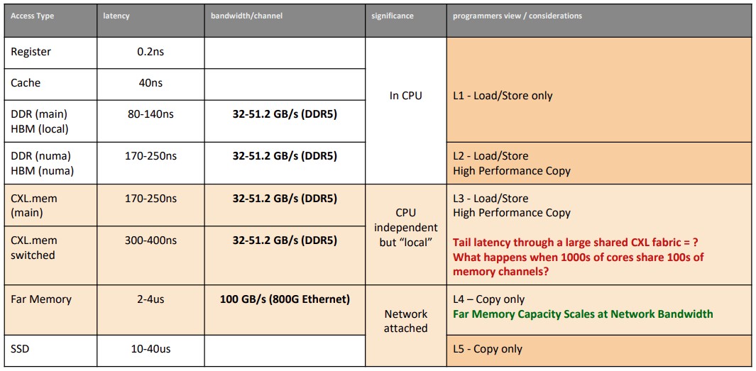
It is that CXL.mem switched memory tier in the storage hierarchy that we are simultaneously excited about with CXL 3.0 and also worried about because this could be the next huge bottleneck in a distributed system design. If you move a lot of the memory in systems to a shared pool, that means that servers can literally share the same copy of the data, but the very act of sharing might add huge latency as more and more nodes try to access it. Multipathing, adaptive routing, and congestion control will all be needed, clearly. And these things have tended to suck in HPC switching stacks, and they suck so bad that hyperscalers use Clos network topologies and massively overprovision their networks to avoid such contention as much as possible.
We are very interested in seeing how the ACF chip will bring memory pooling and sharing in a fashion of the future CXL 3.0 to bear. The devil is definitely in the details here.
But here is the upside of that effort, according to Mukherjee, who showed off the unified memory fabric that is clearly inspired by the UCS system at Cisco but working at the memory and storage layers as well as the Ethernet fabric layers between server nodes. This is, in a very real sense, UCS 2.0, or even UCS the way Cisco no doubt wishes it could have done. (But remember, PCI-Express was stuck at very slow speeds back then.) Take a look:
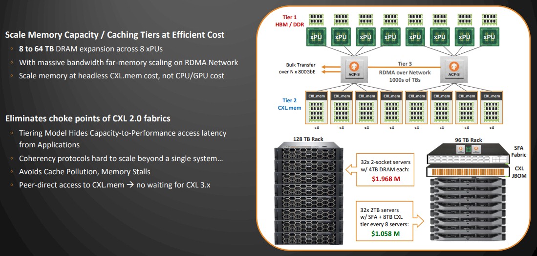
Isn’t that pretty? It’s like NVLink for everyone, for every compute engine, and CXL 3.0 memory sharing, and converged Ethernet NIC and top of rack switching – all at the same time. We will see how the bandwidth and latencies all compare when the ACF silicon actually launches.
(Note: The SFA in the chart above is supposed to be ACF; that is a reference to an earlier name for the Enfabrica chip.)
In the example shown above, the memory and pricing is for CPU-only nodes with DRAM memory, but you can easily make a similar stack with a mix of CPUs and GPUs and their local memory plus shared CXL memory pools as shown with the CPU-only setup. The shared CXL memory will save money and, provided there is not contention on the ACF fabric, allow for datasets to be shared and not have to be copied. Think of this as a rack-scale pod of compute. We are fairly certain that Enfabrica will be able to scale across multiple racks to build bigger pods, but Sankar and Mukherjee are not talking about that yet.
Looking ahead, we can also see a time when you might cut the local memory off the XPUs and only use CXL fabric memory to feed the devices. But we are getting ahead of ourselves. That feels like a PCI-Express 7.0 and CXL 4.0 stop on the roadmap to us. But imagine just having raw CPUs and GPUs on tiny packages, interlinked with ACFs to giant pools of CXL DRAM and maybe even adjacent HBM memory pools. With a high enough radix on the ACF, you could lag multiple pipes together to create a high bandwidth and fairly high capacity memory unit. Probably not as capable as HBM4 or HBM5, but probably a hell of a lot cheaper.

Enfabrica Nabs $125 Million To Ramp Networking Godbox
For the past decade or so, we have been convinced by quite a large number of IT suppliers that security functions, network and storage virtualization functions, and even the server virtualization hypervisor for carving up compute itself should be offloaded from servers to intermediaries somewhat illogically called data processing units, …
Enfabrica Takes On Hyperdistributed I/O Bottlenecks
Not so very long ago, distributed computing meant clustering together a bunch of cheap X86 servers and equipping them with some form of middleware that allowed for work to be distributed across hundreds to thousands to sometimes tens of thousands of nodes. Such scale-out approaches, which added complexity to the …
Looks very much like what the Dr. ordered — for disaggregated composable high-performance computing! The composition of the ACF’s secret sauce should determine whether it blends best with APU-style dish trays, or with raw GPU recipes, as you suggest (“just networking trays of GPUs to ACFs […]”) — say Worcestershire/tobasco vs fish/cephalopod sauce. I would imagine, for example, that POWER10-like cephalopodic SerDes ingedients (in the ACF), would promote summoning of flexible memory access kung-fu spirits, that would pair well with trays of raw GPUs. A more bland sauce, while still tasty, may on the other hand be somewhat limited to karate-like emanations, that best harmonize with slicing and dicing of linear and blocky preparations, and thus require some tentacular pick-me-up ahead of the Gustative PU. Irrespective, this is a tasty proposition from Enfabrica!
This just like old time Maxcore https://electronicsmaker.com/maxcore-platform, try to bridge the PCIe/Ethernet, also include the CXL for memory. How to benifit to Chatgpt training will be tricky. Last time, the PCIe and Ethernet combine for OVS/NFV workload didn’t make any much noise.
Good point! I do think however that the contemporary zeitgeist (from DOE and other federal funding efforts) favors hub-and-spoke networks of independently upgradable cephalopods (squids), for which this type of rack appears particularly well suited.