
For the past decade or so, we have been convinced by quite a large number of IT suppliers that security functions, network and storage virtualization functions, and even the server virtualization hypervisor for carving up compute itself should be offloaded from servers to intermediaries somewhat illogically called data processing units, or DPUs.
And so the race has been on by networking companies and startups as well as hyperscalers and cloud builders to build DPUs, which are extremely SmartNICs with their own compute for data pre-processing and post-processing, to plug into servers so the very expensive CPUs can just do the serial processing application and middleware work that is their raison d’etre.
But. What if all of this stuff really belongs in the network itself? Especially when there are so many collective operations that need to be done in distributed computing and especially with memory now also being distributed across the network like compute and storage. . . .
This is not precisely what Enfabrica, a startup founded in 2020 by Rochan Sankar, its chief executive officer, Shrijeet Mukherjee, its chief development officer, who both have long histories in datacenter networking, are doing, but it is creating a composable fabric for memory and I/O and we think it is perhaps inevitable that this ASIC will also eventually include all of the DPU functions it does not already perform.
Not to give Sankar and Mukherjee more than what they already have to do. Enfabrica now has over a hundred engineers and that are creating what the founders call an Accelerated Compute Fabric Switch, or ACF-S, that disaggregates and composes CXL memory as well as providing connectivity and composability for CPUs, GPUs, and NVM-Express flash. The ACF-S basically converges the Ethernet switch and its NIC down to a single piece of silicon, and so if you believe in DPU offload, well, then the kind of thing we are talking about is all but inevitable for Enfabrica.
The first generation of the ACF-S silicon, codenamed “Millennium,” is a good place to start. Enfabrica has just raked in $125 million in its oversubscribed Series B funding round to help the company ramp up engineering and sales as it gets ready for a big product push in 2024.
Here is what the Millennium chip looks like conceptually:
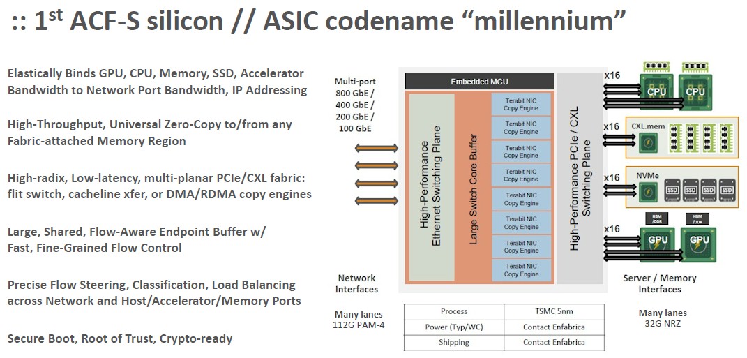
See what we mean? Put on some accelerator engines for encryption, decryption, compression, hashing, and a bunch of cores for running a hypervisor and other pre-processing and post-processing algorithms for applications on the server, and BAM! You got yourself a Godbox. And this Godbox can eliminate a lot of the in-server and cross-server interconnects that are used within a datacenter rack these days – including Nvidia’s NVLink fabric or AMD’s Infinity Fabric, just to name two, although you will be hard-pressed to get Sankar and Mukherjee to say that now that Nvidia is one of the investors in that Series B funding round.
Enfabrica raised its $50 million Series A round in June 2021, a little more than a year after it was founded, and that is when it started talking about “the $10 billion I/O problem” in the datacenter and pointed out all of the problems with the way compute, memory, and I/O were being networked.
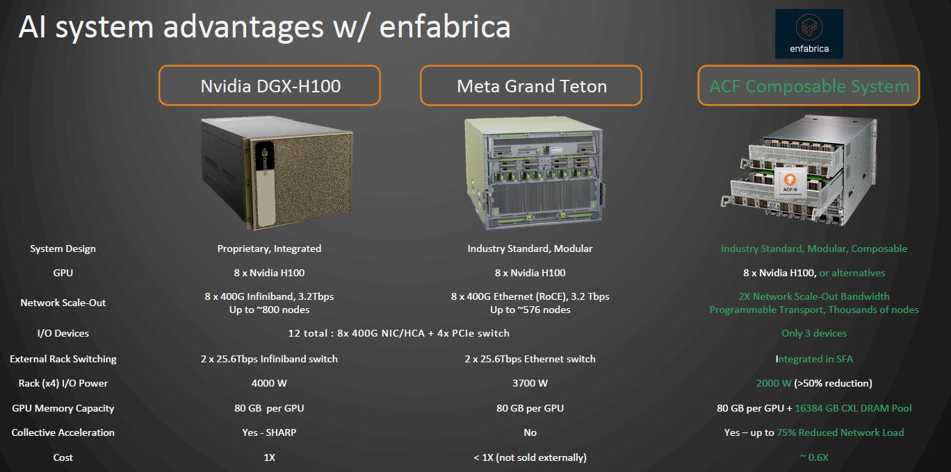
In March this year, when the ACF-S silicon was finally announced, here is how Enfabrica positioned itself at the heart of AI training systems, and very clearly, the company is suggesting it can create a composable GPU server that is better than the systems created by Nvidia and Meta Platforms and that it can further extend that composability out across a network of ACF-S devices to create a larger, virtual pool of compute and memory than either Nvidia or Meta Platforms are doing. Cutting out 40 percent of the cost of these AI systems, as Enfabrica is suggesting it can do, is an important thing when putting together a machine that can train a large language models with 1 trillion or so parameters can cost around $1 billion.
With the Series B funding, the Enfabrica sales pitch is being refined somewhat, with the company positioning its ACF-S devices as a middle tier of networking and memory access for AI clusters, like this:
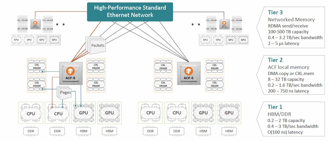
This is an approach that Nvidia can get behind, although we would point out that the advent of its “Grace” CPU was not just to get rid of X86 hosts its in DGX and HGX systems, but to provide a tightly coupled LPDDR memory subsystem as adjunct memory for a “Hopper” H100 GPU accelerator. However, what Enfabrica is doing can be applied to any PCI-Express accelerator, Nvidia or not, GPU or not. And it helps deal with the memory capacity issue that is binding up AI workloads. This doesn’t really help the bandwidth issue for memory on the GPU hosts, but it does mean that a pool of GPUs inside of an enclosure can share memory inside of the nodes and a hierarchy of ACF-S devices can create a fabric for this memory pool – all done before the CXL 3.0 protocol is actually in the field, mind you – to be shared more widely across a large cluster of GPU nodes.
Or, if you just want to use Grace-Hopper superchips, you can do that too, Sankar reminded us, like this:
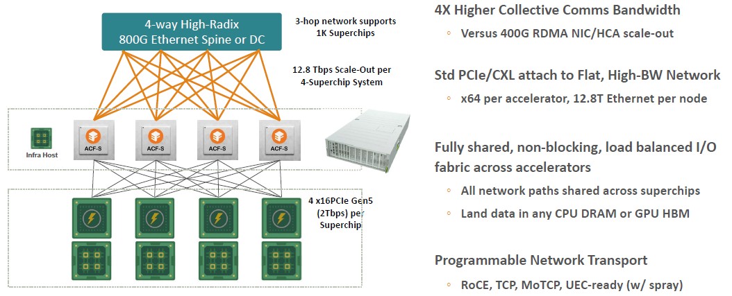
With a leaf/spine network, with an 800 Gb/sec Ethernet switch being the spine and an ACF-S devices being the leaf, up to 1,000 Grace-Hopper devices can be supported in a three-hop network. That is a pretty respectable AI supercomputer. The Nvidia DXG GH100 cluster tops out at 256 of these Grace-Hopper superchips. Add another hop in the spine network and you can scale it a lot further, but this also adds network latency.
“The idea with a platform like this is that we can build a datacenter-scale AI network that appropriately tiers and disaggregates the resources in such a way that it not only optimizes performance, but composability,” Sankar tells The Next Platform. “Right now, everything has been packed into these extremely large, extremely expensive pieces of equipment. But we create a black box that enables datacenter-wide composability. So varying the number of GPUs, varying the number of CPUs, as we need to do for AI inferencing versus AI training, can be done. Depending on the choice of the GPU, you might have a different ratio of memory to compute flops. Our system enables the tiering of memory closest to the GPU, all the way to what we would call farm memory that ingests and moves data. When you think of the various amounts of things that go on in the AI cluster, it’s not just the inner loop of matrix multiplication math. It’s serving context storage, it is pre-processing, it’s labeling, it’s checkpointing. For all of those functions, where does that stuff go? It needs like big swaths of fast storage. And right now, GPUs are operating like an L1 cache with everything in HBM memory. By contrast, we are bringing an ability to move and store data in extraordinarily flexible and performant ways.”
For instance, imagine you needed to create a less expensive inference engine for LLMs. You might do something like this:
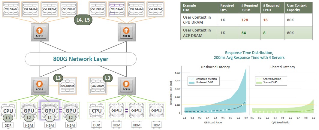
In the setup above, the idea is to drive 1,000 queries per second on a large language model like ChatGPT-4, and to do so with an average response time of 200 milliseconds sand storing 80,000 parameters of user context in the model. As you can see, Enfabrica thinks it can drive that inference with half the number of CPUs and GPUs by hanging CXL DRAM off the ACF-S devices in different parts of the network. Memory is a lot cheaper than GPUs are right now – that is for sure.
That is all conceptual. What Sankar really wanted to show off to us is real hardware, starting with am ACF-S networking node:
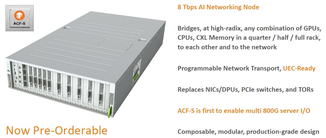
We can see that the ACF-S replaces NICs, but we are uncertain to what extent it can replace true, full-blown DPUs. But clearly, in the longest of runs, as we pointed out, the ACF-S should do so and this should save companies from having to buy a DPU for each server.
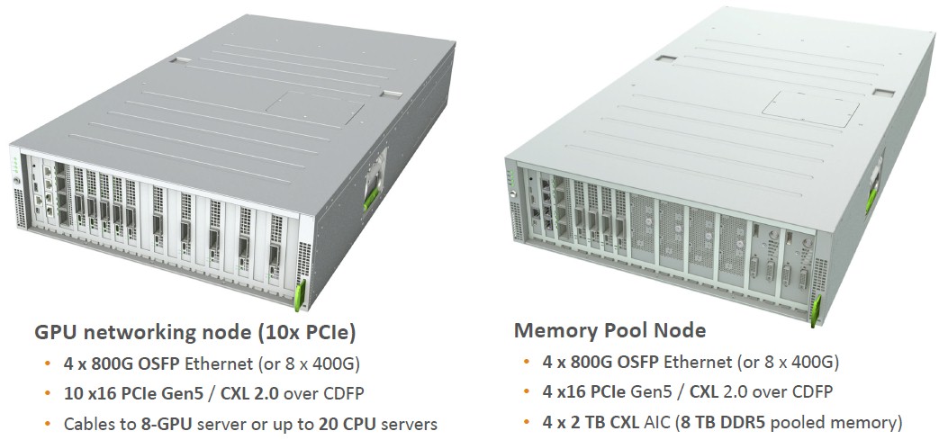
The ACF-S system can be configured as a GPU networking node, hosting up to ten PCI-Express 5.0 x16 devices and up to four 800 Gb/sec or eight 400 Gb/sec. It has enough power to host up to eight GPU accelerators or up to 20 CPUs in server sleds.
As a memory pooling node, the ACF-S system can have up to four 2 TB CXL add-in cards, with a total of 8 TB of DDR5 memory, with four PCI-Express 5.0 x16 ports out to servers and the same four 800 Gb/sec or eight 400 Gb/sec Ethernet ports coming out to the network.
Here is a drilldown on the GPU/CPU node configuration, which in this case shows two ACF-S ASICs, eight GPUs, and what looks like a pair of host CPU cards:
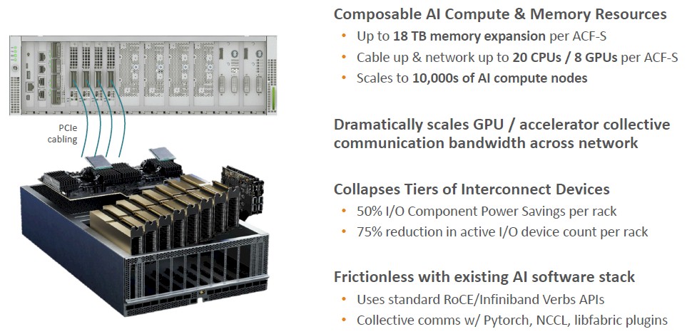
That 75 percent reduction in I/O components and 50 percent reduction in I/O component power per rack is a big deal.
So, it is no wonder that Nvidia is one of the investors in the Series B funding for Enfabrica. Nvidia is spreading its cash around to all kinds of startups, just like Intel had done in the prior two decades. And that is to keep your friends close, and your potential rivals even closer. Nvidia was not the lead investor. That was Atreides Management, with support from existing investor Sutter Hill Ventures. IAG Capital Partners, Liberty Global Ventures, Valor Equity Partners, Infinitum Partners, and Alumni Ventures all kicked in some dough, too. Enfabrica says that the Series B round increased its valuation by 5X, but did not say what that valuation was.

Enfabrica Converges Extended Memory And I/O Down To One Chip
Disaggregation means a lot of things, but the one thing that it most certainly does not mean is that every little thing in a system necessarily has to be smashed apart and then put back together in a composable ways. Sometimes, it makes sense to aggregate devices in new and …
Hell Freezes Over: Cisco And Nvidia Cross-Pollenate AI Networking
UPDATED Networking giant Cisco Systems and AI platform provider Nvidia have hammered out a deal to mix and match each other’s technologies to create a broader set of AI networking options for their respective and – importantly, prospective – customers. Nvidia has been a competitor of Cisco’s in the datacenter …
Pushing AI System Cooling To The Limits Without Immersion
Here is a question for you. What is harder to get right now: 1,665 of Nvidia’s “Blackwell” B200 GPU compute engines or 10 megawatts of power for a four year contract in the Northeast region of the United States? Without question, it is the latter, not the former, and both …
That’s quite the squid giant axon right there! Congrats to Enfabrica on this series B funding for its innovative and impressive cephalopod-inspired Accelerated Compute Fabric Switch (ACF-S)!
Farming, ingesting, moving, and storing data through disaggregated heterogeneous subsystems, composed efficiently by flexible and performant tentacles, is quite the ExaCthulhu ticket these days (perfect for hubbing-and-spoking too).
I do wonder however, in an almost tongue-in-cheek Burning Man extremophile Triop kind-of way, of the extent to which an ansible puppet chef terraform salt might play a role in orchestrating the related compositions, or if an altogether different breed of spirits is to be summoned for this purpose (or none at all)?
I think you just shake it by the shoulders and say, “Compose yourself.” And then it does.
Biodynamic composition articulated over smart limbs … nice! %^b
Nice .. but what problem are you solving 🙁
Seem like another grave for good money
Well, the functionality has to be somewhere, it can’t be implememted in the copper or glass fibre network cables. So it’s gotta be in a box. IMO the functionality is become somewhat comoditized, so the fight becomes about “my form factor is better than yours”.
The DPU scheme though, that is a pretty cynical “solution”… buy a server and then buy expensive PCIe AICs to offload the work from the server to the server’s AICs. I suppose Jen Sen had to find *some* justification for trying to acquire ARM. But a bunch of tech sites (STH!) really fell for it hard.
Just wonder how to plug a GPU card or CPU card or MEM CARD into ACF BOX ? How to install them together in a RACK ?