

AMD president and chief executive officer Lisa Su is fond of saying that the road to Rome goes through Naples as a way of reminding everyone that they can’t sit on the sidelines and wait for the second generation “Rome” Epyc processors to come to market in 2019. They have to make use of the “Naples” first generation Epycs and do their system design and software testing there so they can be better ready for the Rome chips and prepared better still for the third generation “Milan” chips based on the “Zen 3” cores coming sometime in late 2020 or early 2021, depending on how you want to interpret the AMD processor roadmaps.
This is an apt metaphor that AMD uses with its code names, particularly if Sicily is meant to be Intel Xeons in the datacenter and AMD is gradually building up for a big kick. (You can almost hear someone scream “GOAL!”) Because indeed, there is a road that goes from Naples to Rome, the E45, and then there is another one that links Rome to Milan, the E35. So technically, there are two roads and they go through Rome to connect Naples to Milan. And Rome is most definitely the most important of these, both for Italy in terms of its cities and for AMD in terms of its X86 server chips. Everything will turn on Rome and the legions of servers that, AMD hopes, will be built from them to conquer the Xeon-dominated datacenter.
At the Next Horizon event in San Francisco today, AMD’s top brass revealed some of the specs and competitive analysis for its forthcoming Rome Epyc processors and “Vega 20” Radeon GPUs that will be deployed in its Radeon Instinct MI60 GPU accelerators. We will be covering the CPUs and GPUs separately, but suffice it to say that for the first time in a very long time, it looks like AMD will be able to stand toe-to-toe with Intel in CPUs and Nvidia in GPUs, and it will be very interesting indeed to see how the market reacts to this and how Intel and Nvidia counteract AMD’s move.
Rome Wasn’t Built In A Day, Nor Was It Sacked That Fast
Intel has already reacted to the future Rome chips, which have been sampling for a few months and which ship in 2019, with the 48-core “Cascade Lake AP” chip that the company released some information about just ahead of AMD’s shindig. (Because it be like that sometimes.)
There was chatter that the Rome Epyc chips might have 48 cores, and then other talk that it would have 64 cores, and this seems to settle the matter, and it looks like the 48 core chip might have been an interim Naples kicker etched in 14 nanometer processes (perhaps with two more 8-core dies per socket) that AMD was supposedly kicking around and that was not on any public roadmaps we have seen. Su confirmed today that the Rome processor would indeed have 64 cores in its socket, and AMD’s chip designers have taken its interconnected chiplet concept – one that will be the future of processing engines of all kinds as Moore’s Law runs out of gas – up another notch by mixing chips of two different process nodes on the same package to create the Rome Epycs.
To be precise, AMD has taken all of the I/O and memory controllers of the Zen 2 cores and pulled them into a single chip that sits at the center of the Rome package; this I/O and memory chip is implemented in well understood and better suited 14 nanometer processes mostly because I/O signally scales down badly as you try to shrink it. (We expect for switch ASIC makers to start breaking out SerDes communications circuits from data flow engines in much the same way and for exactly the same reasons, but as far as we know, they have not done so yet.)
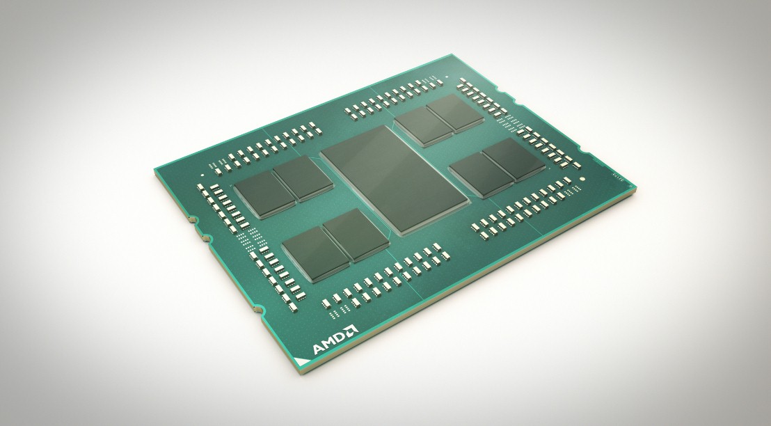
The compute core blocks, on the other hand, scale down really well from 14 nanometers to 7 nanometers. In this case, it looks like four distinct blocks of cores, comprised of eight total eight-core chiplets based on the Zen 2 cores, are on the Rome package and they link to this I/O hub chip through an improved Infinity Fabric, itself based on PCI-Express 4.0 signaling. Here is how the Naples and Rome chips map out, conceptually:
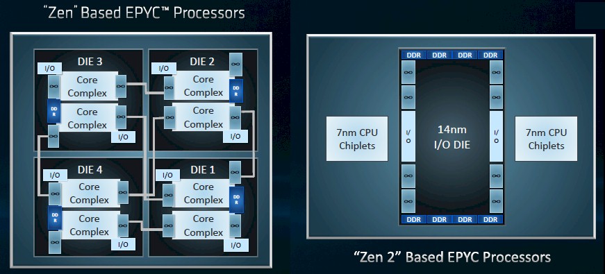
The way the architecture works is that PCI-Express 4.0 gives Infinity Fabric twice the bandwidth, and the change in topology by moving to a central I/O and memory hub eliminates one layer of NUMA hopping, which in turn improves the latency of the in-socket interconnect. To put it simply, more code will run better on Rome than did on Naples, and that is because of the underlying hardware architecture but also because of the work that has been done with the Linux and Windows Server schedulers to be aware of the Naples and Rome chip NUMA topologies.
The other big change with any processor architecture is the amount of instructions per clock, or IPC, that can be gained just from architectural improvements.
With Intel and its tick-tock method of improving performance of Xeons, when it was making a manufacturing process node change (a tick), the architectural enhancements were fairly modest – sometimes nothing at all like the bump to the “Westmere” Xeons, sometimes 4 percent or 5 percent – and with the tock architectural changes, integer performance might go up by around 10 percent in the core. The AVX vector math units were on their performance ramp schedule, and Intel doubled the width of the vector units every now and then, from 128-bit to 256-bit to 512-bit most recently, doubling the floating point performance every time. (There are some scheduling issues with the 512-bit AVX-512 on the “Skylake” Xeons that sometimes means they don’t quite get enough work to both units, so it is sometimes less than 2X the performance of the AVX2 vector units.)
By moving from the “Dozer” cores used in the old Opteron chips from many years ago now to the Zen core, AMD delivered an impressive 52 percent jump in IPC for its server and client processors, a big jump indeed but at least half of that you might have expected in the four generations of Opteron processors that could have been launched over the intervening years and were not. Manufacturing nodes would have given such mythical chips plenty of added throughput. So in a sense, AMD is just catching up. The point is, it is not just catching up to where it could have been, but it is leapfrogging Intel thanks to the advantage that 7 nanometer manufacturing gives over the enhanced 14 nanometer technology that Intel has to use for servers until early 2020 when “Ice Lake” Xeons come to market.
Mark Papermaster, chief technology officer at AMD, did not say how much IPC to expect in the jump from the Zen 1 cores used in the Naples Epyc chips to the Zen 2 cores used in the Rome chips, but a bunch of us were sitting around talking shop around the lunch table here and we don’t expect for IPC to increase in the jump from Zen 1 to Zen 2 by more than 10 percent to 15 percent. Given the typical Intel Xeon changes in IPC, this is still huge by comparison, of course. Officially, the IPC increase is more like 29 percent, according to the fine print in the AMD presentations, which are based on DKERN and RSA microbenchmarks and which measured at 4.53 IPC for the Zen 2 core versus 3.5 IPC for the Zen 1 core. But again, we were talking about integer performance in the Intel examples.
Couple that IPC increase with the doubling of core count per socket, the IPC uplift is basically compensating for the slowing of clock speeds that is necessary as more cores are added to chiplets and therefore to the Rome package. (We will talk more about that in a minute.)
Papermaster did not give out the feeds and speeds of all of the architectural enhancements, and he did not disparage the significant manufacturing node advantage that AMD can hold is its foundry partner, Taiwan Semiconductor Manufacturing Corp, can make good on its promises to deliver Rome chips next year. (We still think earlier, to the cloud builders and hyperscalers, rather than later in the year.) Just shifting from 14 nanometers to 7 nanometers would allow for a chip to have twice the transistor density at half the power consumption and deliver about a 25 percent performance boost in the performance of those transistors at the same time. But AMD is going with a hybrid process that freezes the I/O and memory controllers at 14 nanometers – and also locks them into 128 PCI-Express lanes of traffic and eight DDR4 memory controllers, both of which are necessary to maintain the socket compatibility that AMD has promised between Naples and Rome systems. So until customers want to buy 256 GB DDR4 memory sticks, the top end memory per socket of Naples and Rome will stay at 2 TB per socket.
In addition to the other architectural changes mentioned above, the Rome chips will sport an improved branch predictor, better instruction pre-fetching, a larger op cache, and a re-optimized instruction cache.
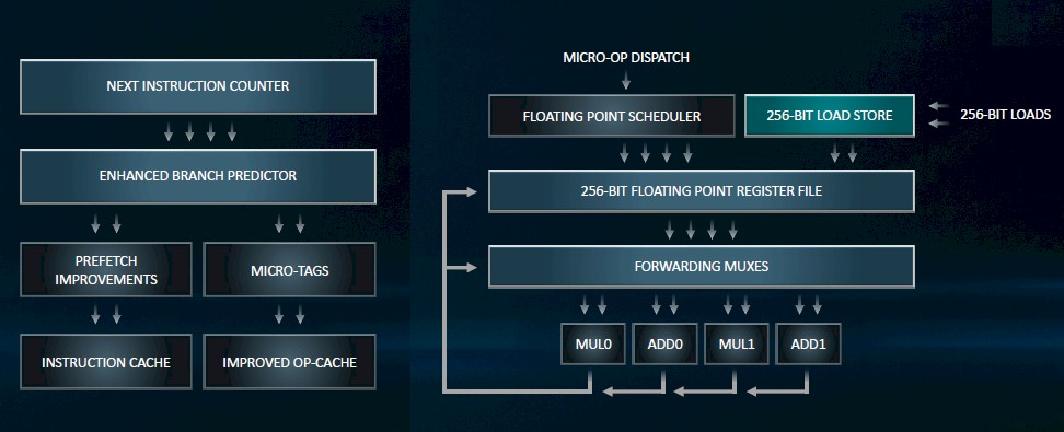
The width of the floating point units with Rome are doubled to 256 bits, and the bandwidth into and out of the load/store units are also doubled with 256-bit data paths and floating point registers are also doubled up in size to 256 bits. The upshot is that with twice as many cores and vector units that are twice as wide, floating point performance on Rome will be 4X that of Naples, and integer performance will be 2X.
“I have been in the semiconductor business a long time and you just don’t get 2X generational performance enhancements,” Su said with a laugh. (Well, actually, now you do.)
To show off a bit on the performance, Su showed off a system running the ResNet-50 image recognition benchmark on a machine learning training run that paired a Rome processor with a single “Vega 20” GPU accelerator against a single Naples Epyc 7601 processor with a Radeon Instinct MI25 accelerator, and the forthcoming machine ran the test more than twice as fast. AMD also demonstrated a benchmark using the C-RAY ray tracing benchmark, this time pitting a two-socket Intel “Skylake” Xeon SP-8180M, each with 28 cores, against a single-socket Rome machine with 64 cores and a two-socket AMD machine using 32-core Naples Epyc 7601 processors. In the test run we saw, the Skylake machine could do the various renderings in 30.4 seconds, the Rome machine could do it in 27.1 seconds, and the Naples machine could do it in 28.4 seconds.
The advantage is going to Rome, clearly, especially when you consider that two of those Intel Skylakes list for over $26,000 and the hyperscalers and cloud builders, who get the deepest discounts, are maybe getting 25 percent to 30 percent off, not the 50 percent they are used to. It is actually hard to figure precisely where AMD should set its price for the top-end Rome part. Is $8,400, which is twice what a Naples Epyc 7601 costs, too high or not high enough?


Intel “AMD is just using glue techniques for their CPU production…”
[Troll Faced] AMD: “Glue ALL THE THINGS!!!”
“4.53 IPC for the Zen 2 core versus 3.5 IPC for the Zen 1 core.”
Do you mean bulldozer vs Zen 1? Where does the 29% ipc increase zen1 -> zen 2 come from?
Do the math. 4.53 is 29% larger than 3.5
If you read the article you would know that IPC has increased due to a node shrink, and various architectural improvements.
@Author,
With 7nm, 0.5x the power and 2x the density (core count), so 2x the performance with 1x the power per package.
2x the performance per watt (from 7nm), but 1x the IPC performance with all the architecture improvements?
@David
“2x the performance per watt (from 7nm), but 1x the IPC performance with all the architecture improvements?”
You don’t get perfect performance scaling by adding more cores. Without IPC improvements, the performance gains would be around 1.7x rather than 2x. I wouldn’t be surprised if Zen 2 delivers IPC gains per core of around 15% at the very least. Maybe more.
@Lin,
Thanks.
Real competition for dual-CPU Rome servers will be with quad-CPU Xeon Gold servers (not with anything like 2×8180 which doesn’t stand a chance). And then it’ll get much more competitive due to higher number of DIMM sockets (48 with 3TB RAM size limit when using reasonably priced 64GB DIMMs vs 32 and 2TB for dual-CPU Rome – since prices for 128GB DIMMs remain insane) and comparable (unlike for dual-Xeon) number of PCIe lanes (after adjusting for speed difference between PCIe 3.0 and 4.0). It really depends on how AMD and Intel will price their CPUs by the time Rome CPUs are actually available as well as what kind of security issues will be unresolved for each.