

Incremental change is the secret to the success of the human race, and it is also its most difficult aspect in some regards. We need to move things ahead, but at the same time we cannot break what works. And this is how we end up with ever more ornate architectures in all kinds of systems ranging from way down inside the CPU socket on out to the hyperscale datacenter and to the networks of politics, economics, and culture that enmesh the Earth.
The X86 architecture embodied in the Intel Pentium and Xeon server processors is incredibly sophisticated, and has been continually adapted to suit the processing needs of a widening array of applications that are themselves increasing in complexity. There are not many businesses that are easy these days, but it would be tougher to find one more difficult than designing CPUs and the manufacturing processes that keep them evolving – or one more financially rewarding for those who can pull this engineering feat off generation after generation.
With the “Cascade Lake” Xeon SP processors announced two weeks ago, Intel has once again moved the architecture forward, perhaps by dozens of inches instead of yards because it is currently in a holding pattern using its 14 nanometer wafer etching. But the changes Intel made in the processors and its delivery of “Apache Pass” Optane Persistent Memory Modules, which bring 3D XPoint to the DDR4 main memory form factor, are in important ways that will make the processors appealing to customers even though there is a “Cooper Lake” Xeon SP kicker with some tweaks for machine learning workloads right around the corner and “Ice Lake” Xeon SPs with a new architecture as well as a much-anticipated 10 nanometer wafer baking process coming at the end of this year with a ramp in 2020.
The datacenter has changed a lot since the “Nehalem” Xeon 5500 processors were launched by Intel as AMD was still competing strongly in the glass house and, frankly, the public cloud business was tiny and the hyperscalers did not have such a large impact on the systems business as they do today.
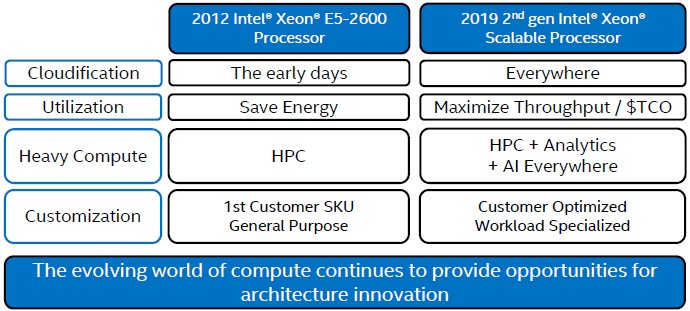
In a presentation going over the finer points of the Cascade Lake Xeon SP, Ian Steiner, principal engineer and the lead architect on the processors and a power and performance architect on all the Xeons since the Nehalems, drew the line in his architectural comparisons from the “Sandy Bridge” Xeon E5-2600 processors launched in March 2012, which we was an important leap in architecture for Intel and which, by the way, came after some delays due to issues with the design and the 32 nanometer manufacturing processes of the device, whose top end part had 2.26 billion transistors and cores. The Skylake and Cascade Lake Xeon SP processors, with those refined 14 nanometer processors, cram 28 cores plus a whole lot of “uncore” circuitry with a total of 8 billion transistors. But the differences in the market are more profound than these basic feeds and speeds imply, as Steiner showed:
“Things have changed a lot since then,” explained Steiner in a briefing going over the architecture of the Cascade Lake processor. “The public cloud was just getting started. We had a lot of customers that were really worried about energy savings and SPEC power and other measurements, but today what customers are really nagging us about is how we they can improve the throughput of their systems and really take advantage of the investments that we are all making. So a lot of the capabilities we are putting into our systems are less about running traditional benchmarks and how we can use a system to its peak. I remember reading papers back in 2010 about datacenters running at 20 percent utilization, and if I was a finance guy, that would make me really mad. If customers were really using our systems at 20 percent utilization, we wanted to figure out how to get them to 50 percent, 60 percent, or even 70 percent or 80 percent of their capability. That has been one of our big focuses.”
Steiner also says the nature of high performance computing has changed a lot in those seven years as well. “We are seeing a lot more heavy compute in other parts of the market, and with AI and some other analytics workloads, a lot of those high performance computing characteristics are expanding out to other use cases. This is just getting started now, but we think this is going to continue to expand into the future,” Steiner said. The other big change in the CPU market that Intel has fomented at the urging of its customers – and which goes along with pushing each chip to its full potential – is customization. The first custom Intel CPU was during the Sandy Bridge generation, and now Intel has “just piles” of these, as Steiner put it. And a quick review of the Cascade Lake product line shows how mass customization, with Intel turning all kinds of knobs on the processor to activate or deactivate processor features and cranking up and down the clock speeds to tune performance for specific workloads is the norm. Here is a handy chart that shows a scatter graph of the main SKUs in the Cascade Lake line, what Intel recursively (or repetitively) calls the Scalable Processor portion of the product line:
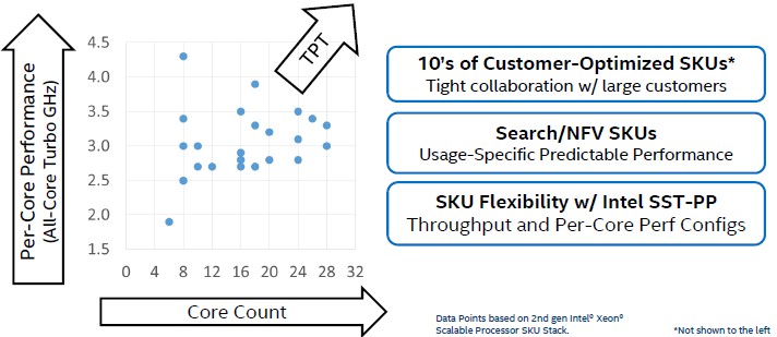
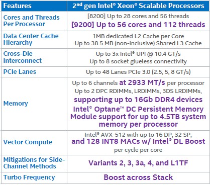
There are 53 standard Cascade Lake Xeon SP parts, including the medium and large memory variants of the Platinum series, and that does not include the custom parts that Intel is still making for OEMs and ODMs for their respective end user customers in the enterprise, HPC, cloud, and hyperscale sectors. As we have pointed out before, there are really three different versions of the Skylake and Cascade Lake Xeon SP processors – Low Core Count (LCC), High Core Count (HCC), and Extreme Core Count (XCC) variants of the Cascade Lake chips, which have 10, 18, and 28 cores maximum respectively.
The Nehalem Xeons from 2009, by contrast, all came from the same die design, all had four cores, all had 8 MB of L3 cache, and they were differentiated predominately on clock speeds, which ranged from 2.26 GHz to 2.93 GHz. The clock speeds have not changed much because of the end of Dennard scaling, which started to breakdown around 2006 or so. As best we can figure, due to changes in the core pipelines, the cache structures, and other tweaks, the instructions per clock (IPC) for integer workloads has increased by 41 percent between the Nehalem and Skylake generations, and given that the Cascade Lake core is a derivative of the Skylake design with security mitigations for Spectre/Meltdown mitigations, tweaks in the vector engines to run 8-bit integer instructions (INT8) for machine learning inference, and changes to allow for Optane PMM memory to run on the systems, we do not think that Intel has changed the IPC for integer jobs running through the core arithmetic logic units (ALUs) moving from Skylake to Cascade Lake. This is what happened when Intel went from four-core Nehalem processors in 2009 to six-core “Westmere” processors in 2011. But Intel did mix up the core counts, clock speeds, thermals, and price points starting with Westmere Xeons, a process that has continued to expand the number of SKUs in the Xeon line since that time.
Intel has been gradually been ramping up memory bandwidth per socket through the combination of adding faster DDR3 and DDR4 memory to the systems as well as more memory controllers per socket, just like other chip makers have been doing.
The Nehalem Xeons had a single memory controller integrated on the die (something that AMD did on the Opterons ahead of Intel with its Xeons) that supported two or three DIMMs for two-socket servers. With the Westmere Xeons, two-socket machines had the same memory controller, but the four-socket variants, the memory controllers could drive four memory slots per socket. With the Sandy Bridge Xeons, the four-socket machines and some two-socket machines had four memory slots on the single controller integrated on the die and others had three memory slots, and this memory scheme remained in place for the follow-on “Ivy Bridge” Xeons in 2013 but Intel doubled up the ring interconnect across the twelve cores on the die and therefore doubled up the memory controllers to a total of two per chip. (Each memory controller had two channels). With the “Haswell” Xeons in 2014, more cores were hung off the pair of rings interconnecting the cores and caches on the die, but the number of memory controllers and memory channels stayed the same as with Ivy Bridge; memory got slightly faster. With the “Broadwell” Xeons in 2016, the rings got bigger again, but the memory stayed put at two controllers and two channels per controller for a total of four channels, with the option of three DDR4 DIMMs per channel running at 1.6 GHz or two DIMMs per channel running at the higher 2.4 GHz clock speed. With the Skylake Xeon SPs in 2017, Intel had two DDR4 memory controllers in the mesh interconnect on the die, with three channels each, and customers could run memory at up to 2.67 GHz, which in theory should have been a big memory bandwidth boost for the Xeon processor, but with only two DIMMs per channel instead of the maximum of three with the Broadwells, it was a wash. All other chips from this generation that matter – IBM Power9, AMD Epyc, and Marvell ThunderX2 – had eight DDR4 memory channels per socket, and thus had a 33 percent bandwidth advantage over the Broadwells and Skylakes at the same memory speeds.
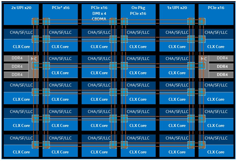
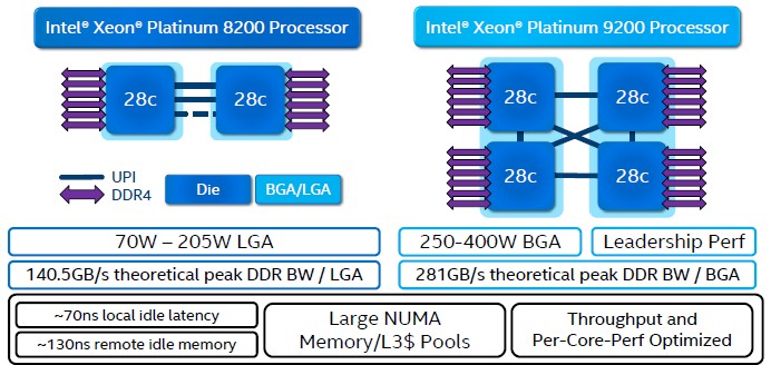
With the Cascade Lake Xeon SP chips just launched, Intel is still at six memory channels per socket for the stock chips, but in the doubled-up Cascade Lake-AP variants, which cram two whole Cascade Lake chips onto the same ball grid array (BGA) surface mounted package (like a giant embedded chip instead of the more standard land grid array (LGA) socket used for server processors. By doing this, Intel can double up what it is putting into a socket, but everyone knows that the two-socket server is really a funky quad-socket server.
If it were not so hard to add more power pins to a socket without having to rejigger the whole chip layout and socket design, Intel would have just added more or beefier memory controllers with the Skylake or Cascade Lake generations, and it looks like we will have to wait until the Ice Lake generation to see that happen. The expectation is for a pair of memory controllers that deliver eight channels per socket and up to two DIMMs per channel, but Intel has not promised anything with Ice Lake as yet. No one else is going to do better than this in 2020, as far as we know, but the memory to core ratios are going to get out of whack if everyone doesn’t start adding more memory. This is why Intel has been pinning its hopes on at least expanding memory capacity per DIMM using 3DXPoint memory, which can boost from a maximum of 768 GB using expensive 128 GB DDR4 DIMMs today across a regular Cascade Lake Xeon SP socket to 4.5 TB in the Platinum versions of the processors with the L memory extensions activated. That fat configuration uses a mix of DDR4 and Optane PMM memory. That configuration uses four 128 GB DDR4 DIMMs and eight 512 GB Optane PMMs, by the way.
The Ever Widening And Finer Graining Vector Engine
With the threat from GPU and to a lesser extent FPGA acceleration using offload approaches, Intel was under threat from in the traditional HPC space as well as in the hyperscale and cloud builder spaces starting back with the Westmere line, and the company reacted by adding more robust floating point capability with successive Xeon generations.
Intel has been focused on scaling up single precision and double precision floating point math on the Xeon line over the past decade, and Steiner admitted that Intel has not been all that interested in bolstering the integer math capabilities of these vector units – that is until machine learning training algorithms, which are using increasingly diminutive integer data formats as time goes by.
The Haswell Xeons had integer math support in its AVX2 vector units, said Steiner, but multiply-accumulate (MAC) operations were not a focus because the 8-bit INT8 format had a very small dynamic range 256 values) versus the 2128 possible values expressed in a single precision FP32 format. But, the precision and dynamic range of INT8 (and some would argue INT4 even) are sufficient for some machine learning training inference routines, so Intel has added this to the AVX-512 vector engines in the Cascade Lake Xeon SP processors. We went into the architecture of the Vector Neural Network Instructions (VNNI), sometimes called Deep Learning Boost (DL Boost), that debut with Cascade Lake back in August 2018, but this chart encapsulates it better:
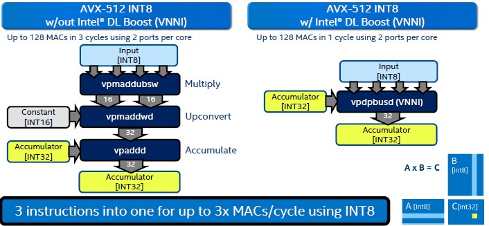
With the Skylake architecture, doing the matrix multiplication of 8-bit integer numbers and accumulating them into a 32-bit integer register (which is necessary to avoid overflows due to the limited range of the 8-bit numbers, something that FP16 or FP32 can handle easily due to the large dynamic range of these data formats). It used to take three steps to do this, and now on Cascade Lake, it only takes one step, and the full AVX-512 unit (meaning both ports are activated) can do 128 of these per clock cycle. This is a lot more than the integer unit in the ALU can handle, at 64-bits a pop.
“Real workloads are probably not going to get 3X performance with DL Boost, but that is okay,” Steiner qualifies. “Our goal was not to say that we are going to maximize peak TOPS on everything. We are trying to build the right primitives into the hardware so that more complex software can get as much performance boost as possible. And that is where you will see a lot of 2X numbers that we were shooting for.”
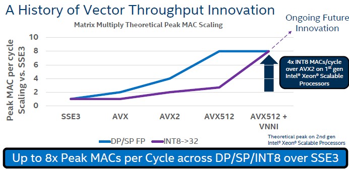
That means getting similar scaling on vector integer formats as has happened with vector floating point formats in the past decade, and here is a handy dandy chart showing the architectural leaps for both floating point and integer in the SIMD engines in the Xeon family over time:
Even though customers are not as obsessed about power consumption as they once were, the team designing Cascade Lake kept an eye on the interplay of power and performance on various inference benchmarks that are commonly used today, and this hairy chart shows how this worked out with DL Boost over the FP32 and the legacy INT8 methodology used in the Skylake Xeons:
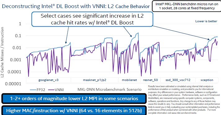
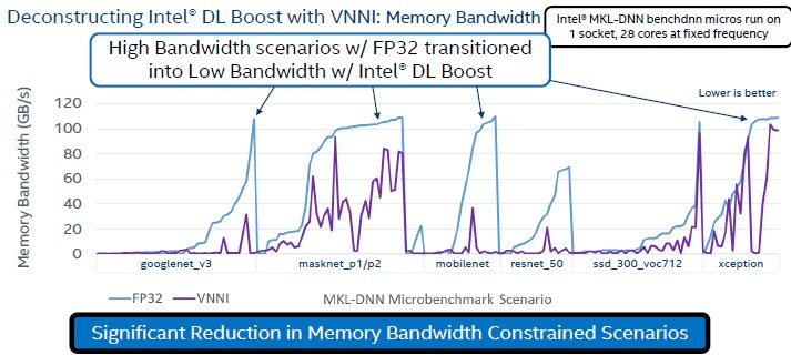
Just moving from FP32 to INT8 on Skylake Xeon SP chips delivered about a 33 percent performance boost in peak MACs per clock cycle, according to Steiner, and the cache and memory bandwidth pressure was alleviated a bit on the processor due to the smaller data size. The INT8 computations on Skylake were also more efficient compared to FP32. Now, moving from that legacy INT8 in the Skylake chips to the DL Boost instructions in the Cascade Lake chips resulted in that 3X increase in peak MACs per clock cycle, and there was no impact on the cache or memory bandwidth (the data formats were the same and the cache hierarchies are the same on the processors), and the power efficiency went up again on these INT8 operations.
That is a general statement, but here is what the comparisons look like if you use real inference workloads:
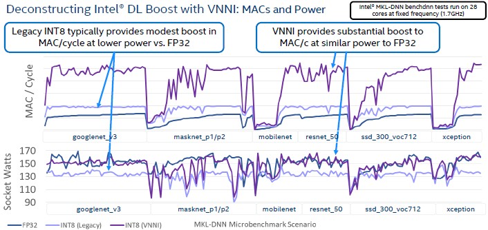
As the chart says, the legacy INT8 approach used a lot less power and gave a modest performance boost, but DL Boost focused on providing more throughput in the same power envelope as doing the same inference in FP32 mode. There may be other workloads that can employ this INT8 – and its companion INT16 – functionality, but thus far none has emerged. But now that the hardware is here, maybe someone will come up with a clever use of it.
The L2 caches, as you can see below, behave a lot better with DL Boost on compared to FP32:
And perhaps equally importantly, the memory bandwidth pressure on the systems settled down moving from FP32 to DL Boost when running inference workloads:
This comes back to the old saw that the hyperscalers and high frequency traders before them and supercomputer customers before even them have been telling system makers for a very long time: Predictable latency and therefore consistent performance on real workloads is much more important than some peak throughput on some theoretical workload.


AMD Finally Breaks The 10 Percent Server Share Barrier
History doesn’t really repeat itself, but it surely does use a lot of synonyms and rhymes, and sometimes, if you listen very closely, you can catch it muttering to itself. It is with this in mind that we contemplate the recent data coming out of Mercury Research, which is the …
NSF Puts $10 Million Into Composable Supercomputer
If they are doing their jobs right, the high performance computing centers around the world in academic and government institutions are supposed to be on the cutting edge of any new technology that boosts the performance of simulation, modeling, analytics, and artificial intelligence. Not the bleeding edge, where the hyperscalers …
Different GPU Horses For Different Datacenter Courses
If the semiconductor business teaches us anything, it is that volumes matter more than architecture. A great design doesn’t mean all that much if the intellectual property in that design can’t be spread across a wide number of customers addressing an even wider array of workloads. How many interesting and …
Thanks for this interesting article. Some number-crunching work has no problem with conventional Ethernet, file storage and per-node memory capacities. The primary bottleneck is main memory bandwidth.
With the code I am working on, a 2 DIMM (DDR4-2666), 6 core i7-8700, with 2MB shared cache per core and ~4GHz clock speed, total throughput is marginally less with 6 active cores than 5. Cache thrashing and RAM bandwidth is the primary bottleneck, and I guess that doubling the cache would lead to only marginal improvements.
The execution speed per instance improves with fewer than 5 cores active, but the overall throughput is important too, and this falls off precipitously below 4 instances.
In evaluating hardware to run this code it suffices to know that a 4GHz well-cached core is seriously limited by 1GHz or less of DIMM. The core GHz vs. core count chart above shows that for this particular number-crunching code, there’s no point going beyond 18 cores per Xeon chip since these are 6 DIMM channel devices with a total of 17.6GHz DIMM bandwidth. IF the inter-chip memory bus was not a bottleneck, then a dual socket 18 core per socket system would be roughly equivalent to nine i7-8700 consumer gaming machines running four instances each. Likewise 32 or 48 core per socket Cascade Lake AP dual chip per BGA behemonths with 12 DIMM channels per socket.
Driving DIMMs requires lots of signal and power “pins” (connections to the CPU chip) with extra power dissipation. The massive two-chip BGA module sounds like a reliability nightmare. The outer solder balls will be subject to metal fatigue due to the size of the BGA. It doesn’t matter how well matched the expansion coefficients of the motherboard and the device are, since the rapid changes in temperature with compute load (400 watts on and off hundreds of thousands of times over several years) will inevitably cause expansion mismatches due to the MB temperature changes lagging those of the device. A single cracked signal solder ball would render the whole motherboard with its soldered on Xeons useless.
I think there is a gap in all existing product lines which would find wide application. Put the CPU chip on a ceramic or silicon interconnect with closely adjacent multilayer high bandwidth memory devices, their top surfaces coplanar so the one heatsink handles them all, similar to the Phi. HBM’s lower latency and higher bandwidth might enable the system to work well with smaller shared L3 caches, depending on the degree to which the software is multithreaded.
For most applications (except massive databases or physics simulation) the HBM would be sufficient, so there would be no need for DIMMs at all, so the power and pins normally devoted to these could be devoted to to the faster, lower power (lower voltage and capacitance), HBM links. A variation would be to add inter-CPU links for multi-socket MBs. Within any reasonable pin and power budget, these would be too slow to match the HBR memory, so there would also be DDR links for massive Optane memory capacity, with the HBM as dozens of GB of L4 cache.
64C/128T are
challenging processors for my algorithms where I’m employing one QWORD bitmap to synchronise CPU function threads, or to aggregate any feature state per CPU.
Strangly I have notice that the count of physical Cores stays below or equal to the architecture length, aka 64 bits.
Beside the HTT/SMT trick, I’m wondering if going to 128 or 256 Phy Core Count will require larger registers size in next gen Processors.
This question matters because I try to employ as much as possible atomic instructions in code (see CoreFreq project in website for those asm usages)