

The changes to the Xeon server chip architecture and the consequent server platforms are going to be a bit thin here in 2018 after a pretty big jump with the “Skylake” Xeon SP processors and the related “Purley” platforms that launched back in July 2017. Intel has been dribbling and drabbling data about the forthcoming “Cascade Lake” Xeon SP kickers to the Skylakes for the past several weeks, and did it again at the Hot Chips conference in Silicon Valley this week.
We did a deep dive on the internal Intel roadmap in late July after the specs on future Xeons and Omni-Path interconnects were accidentally outed in China and then followed up two weeks later with some more crumbs of information from the company’s Data Center Innovation Event. At Hot Chips, Intel’s chip designers provided a little more detail on the new features coming with the Cascade Lake Xeons, including new instructions to accelerate certain aspects of machine learning applications, interfacing with Optane DC persistent memory, which is based on the 3D XPoint memory developed by Intel and partner Micron Technology, and hardware mitigations to plug some of the holes with the Spectre/Meltdown family of speculative execution vulnerabilities that surfaced in January of this year.
Architecturally, if you squint your eyes and look at a Cascade Lake chip, you would see a Skylake chip, and that because not very much is different about them, explained Akhilesh Kumar, principal engineer and manager of the Xeon SP family at Intel.
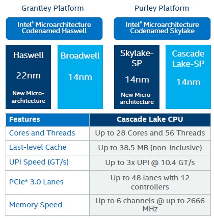
We presume that Intel that will deliver the same LCC, HCC, and XCC variants of the Cascade Lake chips, which have 10, 18, and 28 cores maximum respectively, the same variants it had for the Skylake Xeon SPs. Kumar certainly implied that when he said that the Cascade Lake chips would have the same core counts, cache sizes, and I/O speeds as the Skylake Xeon SPs. The table above confirms the top end configurations, and there is no question that Cascade Lake can be viewed as a special rev of Skylake with some extra stuff woven in.
Cascade Lake will be etched using a slightly more refined 14 nanometer process than is used with the Skylake Xeon SPs, and this will allow some frequencies to be pushed up (our guess is something on the order of 100 MHz to 200 MHz at each SKU, so don’t get too excited) and combined with what Kumar called “specific, targeted improvements along the critical paths in the architecture,” this could boost raw performance a few points on a SKU by SKU basis. All performance improvement is welcome, of course, and particularly if Intel holds the prices steady.
With the increased competition from AMD Epyc, the Arm collective, and IBM Power9, a price increase seems very unlikely and a price decrease (at least at street prices even if list prices remain the same) seems very likely. The important thing is that the Cascade Lake chips will plug into the same sockets as the Skylake SP chips and therefore will present very little engineering work for server makers.
One new thing that is coming with Cascade Lake that was not originally planned for the Skylakes is the Vector Neural Network Instructions, or VNNI for short, which is also something Intel has been calling Deep Learning Boost, too. Before getting into that, Kumar explained how Intel has radically improved the performance on the Skylake processors for machine learning inference work since their debut last year, by a factor of 5.4X, without changing any of the hardware, which is just another way of saying, once again, that machine learning frameworks and algorithms are changing faster than hardware or software engineers can keep up, but every once in a while, the software engineers do catch up and make better use of the hardware and there are big performance gains to be had. Take a look:
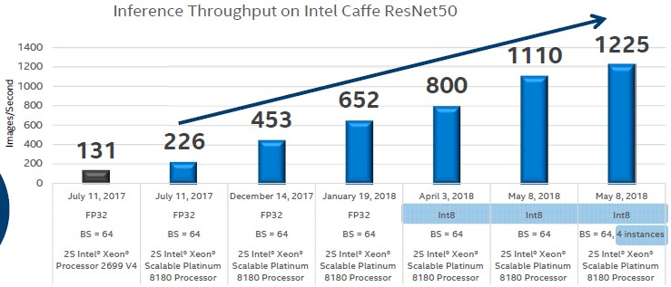
Kumar says that Intel did a lot of work on software libraries and framework optimizations, such as that on the Caffe2 framework running the ResNet50 neural network used for image recognition, to improve performance on the Skylake chips. For inference workloads, moving from 32-bit floating point to 8-bit integer data pipes has helped push Skylake performance, as the chart above shows, by a factor of 4.9X to 1,110 images per second on a two socket machine, and quad pumping the Caffe2 setup with four instances added another 10 percent to 1,225 images per second. If you compare this to the top end “Broadwell” Xeon E5-2699 v4 chip from 2016, the performance boost is more like 9.4X in a little more than a year.
To illustrate the importance of tuning up libraries and frameworks, Kumar trotted out another benchmark, which shows the performance of neural machine translation on Skylake platforms running a German to English translation benchmark on the MxNet benchmark on top of Amazon Web Services C5 instances based on Skylake chips:
![]()
This chart shows the relative performance of the NMT test as batch sizes grow and various optimizations are added to the math kernel libraries and the MxNet framework. The performance increases range from 10X to 14.7X, depending on the batch size and all of the tweaks. And this, said Kumar, was without resorting to jumping from 32-bit floating point to 8-bit integer data sets, which might have boosted performance even further.
“There is a lot of headroom that we can get through software optimizations, and Intel has kept that focus to get these important workloads working well on our CPUs,” said Kumar.
The VNNI instructions are something above and beyond this software work and are done in the microarchitecture.
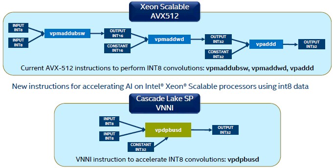
“For Cascade Lake, we looked at some of the critical operations going on in AI and machine learning workloads, and specifically in the convolutions that are a fundamental part of these algorithms,” Kumar explained. “We looked at how the instructions get used for these smaller data types, and then we optimized the instructions. And so for 8-bit and 16-bit integer data types, we defined new instructions that fused three instructions used in 8-bit convolutions and fused two instructions that are used in 16-bit convolutions. By doing that, we have essentially improved performance by 2X to 3X for these data types.”
These VNNI instructions are all done within the AVX-512 vector units. Here is how the 8-bit VNNI instruction works compared to Skylake:
And here is how the 16-bit VNNI instruction works: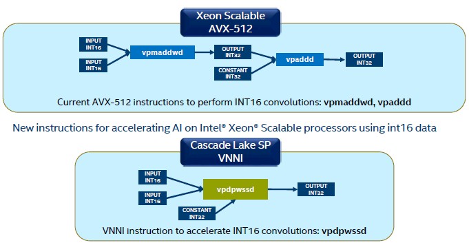
The convolutions, which are essential to machine learning, get processed a lot faster with the VNNI instructions as the data types shift away from 32-bit floating point to either 16-bit integer or 8-bit integer data types, as shown below, which compares Skylake performance on the left with Cascade Lake performance on the right:
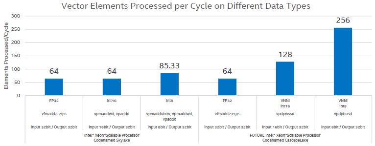
This chart shows performance per cycle per core, Skylake chip versus Cascade Lake chip, and it is important not note that VNNI is just for speeding up convolutions, which is only a part of the machine learning software stack. Still, if you add in the software improvements done during the Skylake generation and then move to Cascade Lake and the new VNNI instructions, you can get about 2X performance on inference at the application level, and if you go back to before the software tweaks, then the jump is nearly 11X over the Skylake processors without all of the goodies. It remains to be seen if the price/performance for inference is better on CPUs, FPGAs, GPUs, or custom ASICs.
The Persistence Of Memory
The other big innovation that is coming with the Cascade Lake Xeon SP chip is integrated support for the Optane DC 3D XPoint persistent memory, something that was part of the Skylake launch and the initial Purley platform when we caught wind of it way back in May 2015. The Optane DC DIMMs, which plug into DDR4 main memory slots and which allow for load/store semantics like main memory, were code named “Apache Pass” and as far as we know, that is still the code name for the Optane memory sticks. They will be available later this year for Purley machines, and only on machines that have Cascade Lake processors; Intel is not opening up the specs for its proprietary tweaks to the DDR4 protocol that allow it to talk to 3D XPoint memory. So forget having this on any other server platform.
The Optane DC memory will come in sticks with 128 GB, 256 GB, and 512 GB capacities, and Intel is not really offering any guidance on the bandwidth, latency, or pricing on Optane DC persistent memory until we get closer to ship date. (Whenever that might be.)
A DDR4 memory channel can have a mix of traditional DRAM and an Optane DC stick hanging off of it, and if customers do such a mix, they will be able to add 3 TB or more of memory per socket to the system. (With 24 memory slots, if half used 64 GB DRAM sticks and half used 256 GB Optane DC sticks – one down from the peak capacities and presumably the highest cost per GB – that is 3.75 TB per socket. Go for the maximums of 128 GB DRAM sticks and 512 GB Optane DC sticks, and you double that up to 7.5 TB per socket. Clearly, with the Purley platform, Intel always wanted to have a mix of DRAM and Optane DC to mitigate against the fact that it only has six memory controllers on the die compared to eight memory controllers for the IBM Power9, AMD Epyc 7000, and Cavium ThunderX2 processors.
There are a lot of ways to access Optane DC memory in a system.
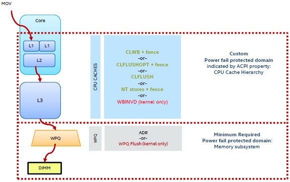
“The minimum thing that we need to do is put the data in the write pending queue,” Kumar said. “But you can do a lot more than that, and if you do that minimum, then software has to take over and essentially make it operate like a storage device to do block transfers or do buffer copies to take advantage of that persistence. That may be fine for some applications, but it doesn’t give you the hooks to take advantage of the load/store and fine granularity effects. You can expand this so an application can write to a single cache line of data and execute certain instructions, like a flush instruction, to that cache line and be treated as persistent. That lets you manage what data gets to be persistent and when that data gets to be persistent.”
Intel is working with the industry to build a technology-independent persistent memory interface that includes more than Intel’s approach to 3D XPoint and will encompass all other kinds of persistent memory.
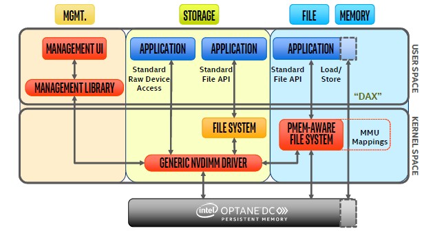
This set of interfaces developed by SNIA for all kinds of non-volatile memory will provide a memory interface or a storage interface or something that smells a little bit like both. There are multiple load/store methods, including using standard memory interfaces in operating systems and exposing the persistent memory as a memory mapped file system. This approach means companies do not have to rewrite their applications. There is also a direct access interface, called DAX, which as the name suggests allows for the access of the persistent memory at the cache line granularity using load/store methods and without having to go through the memory management unit and the kernel space. This is the most exciting new way to access persistent memory, says Kumar. But this will require making applications aware of the DAX interface, and that means rewriting them. Presumably this DAX approach has much lower latency and therefore will be worth the trouble for those applications that are tweaked to take advantage of it.
To make using Optane DC memory easier, Intel has cooked up the Persistent Memory Developer Kit, which has performance tunings and a set of libraries for handling load/stores over the DAX and a set of transaction APIs to manage it. Intel is making the software open source and you can take a gander at it at this link.
At the moment, Intel is positioning the Optane DC DIMMs as a kind of fast flash but slow memory that can nevertheless increase performance on certain workloads. Here is a case in point. Intel loaded up the Apache Cassandra 4.0 distributed file system (created by Facebook) on a Cascade Lake server with DRAM for hot data and with NVM-Express flash SSDs working over the PCI-Express bus for warm data; then it took out the flash SSDs and replaced them with Optane DC memory on the DDR4 memory bus. The quality of service was so much higher on the bus that the machine with Optane DC memory could support 9X the number of read operations per second and 11X more users. Again, we want to do this comparison based on price and performance together.
That leaves the final big set of features for Cascade Lake, and that is the mitigation against Spectre and Meltdown security vulnerabilities. Here is how they line up, and how they are done.
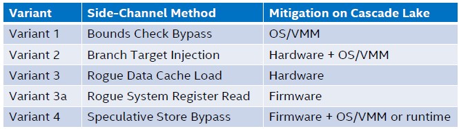
Kumar says that the hardware-assisted mitigation for these vulnerabilities will have a lower impact on performance than the software-based techniques that have been used to date.


Be the first to comment