
With the launch of the “Cascade Lake” processors, the second generation of its Xeon SP family of server CPUs, the fullness of the “Purley” server platform that we heard about way back in 2015 is finally being delivered.
Intel delivered substantial parts of with the first generation “Skylake” Xeon SP chips back in July 2017, but the “Apache Pass” Optane 3D XPoint memory sticks did not make it into Skylake as planned. The Cascade Lake family of chips also include hardware mitigations for the Spectre/Meltdown speculative execution vulnerabilities, which means software patches that often slowed down performance or in some cases required customers to turn off HyperThreading to be fully protected. Many companies obviously did not do this, since there are no known exploits of these vulnerabilities. But some had to, and that had a very big impact on the bin packing of virtual machines on prior Xeon-based systems.
The DLBoost machine learning training modifications to the AVX-512 vector math units, which allow for 8-bit INT8 instructions to be batched up and pushed through these on-chip accelerators and which are also known as the Vector Neural Network Instructions, or VNNI, were slated for the “Ice Lake” Xeons, but have been pulled in to the Cascade Lake generation to help Intel maintain its market share in machine learning inference. The Cascade Lake chips also support DDR4 memory that runs slightly faster than that of the Skylakes, at 2.93 GHz compared to 2.67 GHz.
The point is, now the remaining Purley platform features plus mitigations for Spectre/Meltdown and DLBoost (which was originally expected around 2019 in a different chip) are rolling out with Cascade Lake processors, which plug into the same Socket P sockets that the Skylake processors did, making it a snap for OEMs and ODMs to qualify the new chips and get them in the field.
In addition, in an effort to compete with impending AMD “Rome” Epyc processors, which have more memory controllers and thus more memory bandwidth as well as more cores, and to a lesser extent IBM’s Power9, Marvell’s ThunderX2, and Ampere’s “Skylark” eMAG, Intel is also cramming two whole Cascade Lake processors into a single socket which is calls the Cascade Lake-AP, for short for Advanced Performance. This was not originally part of the Purley plan, and it is not the first time that a chip maker has doubled up chippery inside of a socket when a monolithic part did not give enough oomph of one kind or another.
Intel revealed the Cascade Lake-AP multichip modules back in November, ahead of the Supercomputing 2018 conference and concurrent with the “Next Horizon” datacenter event that AMD was hosting to talk up the Rome Eypc chips, which will have 64 cores and eight memory controllers in a multichip module that can slide right into existing Epyc 7000 systems using the first generation “Naples” chips that AMD launched just ahead of the Intel Skylake chips nearly two years ago. At that time, Intel talked about delivering a doubled-up Cascade Lake that had a total of 48 cores and twelve memory controllers (six per physical chip), but in a new twist announced today, Intel has let the heat dissipation rise and is delivering Cascade Lake-AP chips that scale all the way up to the full complement of 28 cores per chip or 56 cores per socket. The other twist to the Cascade Lake-AP is that it is only available as a single platform from Intel, and as far as we know, no one is able to create their own motherboards for the processors and their custom socket.
Intel first started talking about the tweaks it was making in the Cascade Lake chips last summer at the Hot Chips 30 conference in Silicon Valley, but we had already given you some of the skinny on Intel’s Xeon roadmaps, including a peek at the “Cooper Lake” chips due later this year with support for the bfloat16 floating point format that Google supports in its TPU 3.0 processor and also at the future “Ice Lake” Xeons, which will be the company’s first 10 nanometer chips after many delays that have, quite frankly, given AMD an opening in the X86 server arena. Intel is getting its 10 nanometer act together, and is looking to put out a steady cadence of new cores and new processors, and quite possibly with a chiplet architecture akin to that which both AMD and IBM have used to mitigate risk and avoid waste in their server processors.
This chart nearly sums up the two server platforms and four different Xeon processor families, with their major distinctions:
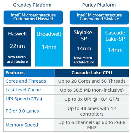
That top memory speed is no longer accurate in the table.
There is not really one Cascade Lake chip, but three, mirroring the approach that Intel used with Skylake Xeon SP processors, which we detailed in our Skylake architecture deep dive back in the summer of 2017. As we expected, Intel is delivering Low Core Count (LCC), High Core Count (HCC), and Extreme Core Count (XCC) variants of the Cascade Lake chips, which have 10, 18, and 28 cores maximum respectively, the same three styles of chips that bear the Skylake name. The chips also have the same L1, L2, and L3 cache sizes and all of the I/O feeds and speeds are the same across the Skylake and Cascade Lake Xeons, and we also expect this to be true with the Cooper Lake Xeon SPs coming later this year. The Cascade Lake and Cooper Lake cores are tweaks of Skylake, not a substantial change to the microarchitecture. Architecturally, this is the pattern we have come to expect from Intel, but we are missing the 10 nanometer process shrink that would have come out this year to allow Intel to boost performance and maybe add some cores as it left the Skylake architecture largely unchanged while paddling over to Ice Lake. Ice Lake, as it turns out, will have both a process shrink to 10 nanometers and a new “Sunny Cove” core coming at the same time, with initial shipments later this year and a ramp in the first half of 2020.
Going forward, Intel will be decoupling features and process so it doesn’t get caught flat-footed as it did by the delay in 10 nanometer processes. Intel has made do with its 14 nanometer processes for Broadwell, Skylake, Cascade Lake, and Cooper Lake Xeons, and clearly it still dominates datacenter compute and is making money hand over fist despite a pause in growth in spending by the hyperscalers and cloud builders in the fourth quarter. So the damage of the 10 nanometer delay has been largely an embarrassment to Intel’s manufacturing operation and nothing more. This is the kind of red face that many server chip makers have worn in the past, so Intel is by no means alone here. The physics of chip etching is getting harder and harder.
The Feeds And Speeds
We will be drilling down into that Cascade Lake-AP platform separately, and also taking a deep dive into the architecture of the Cascade Lake chips, the systems that use them, and how Cascade Lake stacks up to the prior decade’s worth of Xeon server processors. But for now, let’s talk generally about the chip and go through the 53 different commercial variants of the processor that Intel is launching. That’s a good place to start, as always.
Starting with the Skylake Xeon SP processors two years ago, Intel packaged its mainstream and high end Xeon processors in a slightly different way than it had done in the past, with a finer granularity in optional features that were activated or deactivated on different processors. Here is the decoder for the naming conventions of the processors:
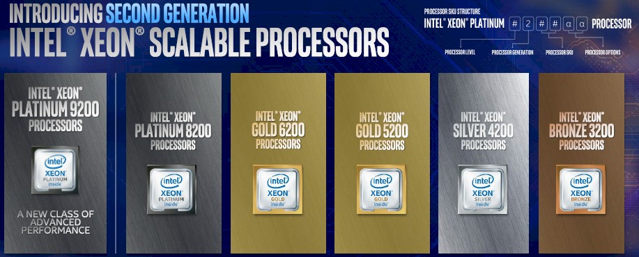
Intel is differentiating the SKUs of the Xeon SP lines not only by the normal four digit numbers that are conventional in the server CPU industry, but by different metal names and their colors to encapsulate and reinforce the distinctions of features between the chips.
With the Cascade Lake Xeon SPs, all of the product numbers have their second digit incremented from a 1 (which designated the first generation Skylake variants) to a 2 (for Cascade Lake). Presumably the Cooper Lake Xeon SPs will have a 3 and the Ice Lake Xeon SPs will have a 4 in that second digit. The initial digit in the Cascade Lake line has also been incremented up to a 9 for the Cascade Lake-AP versions (the 9200 series), which are the versions with two whole chips per socket in a multichip module. The regular single-chip Platinum series is the 8200 series.
The Platinum processors have everything turned on and turned up. The Platinum 9200 series is offered in a four socket system (which is logically really an eight socket system, if you think about it), and the Platinum 8200 series can be used in machines that have two, four, or eight sockets without resorting to external chipsets. The Platinum series, whether 9200 or 8200 series, have up to 28 cores and also have the most I/O with all six DDR4 memory channels and all 48 lanes of PCI-Express 3.0 activated; they also have all three UltraPath Interconnect (UPI) links paths turned on and running at the top speed of 10.4 GT/sec. These Platinum chips also support the fastest DDR4 memory (2.67 GHz in Skylake and 2.93 GHz in Cascade Lake) and have the full AVX-512 vector capability of two fused multiply add (FMA) units activated. There are Platinum SKUs with an M designation that allows the main memory to stretch to 1.5 TB per socket instead of the 768 GB per socket maximum on the other models in the Skylake family. With the Cascade Lake Xeons, the M designation means a chip can support up to 2 TB of system memory per socket and the L designation means it can support up to 4.5 TB per socket. Turbo Boost overclocking and Hyper-Threading simultaneous multithreading of two threads per core are also all activated on the Platinum variants.
The Gold variants of the Cascade Lake Xeon SPs come in two flavors: the 6200 series and the 5100 series. The higher end Gold 6200 supports up to 24 cores (up from 22 cores with the Skylake 6100 series) and can be plugged into machines with two sockets or four sockets; they also have three UPI links per socket running at the 10.4 GT/sec rate. They also have the fastest DDR4 memory and have full AVX-512 support with those two FMAs fired up.
With the Gold 5200 series has a maximum of 18 cores (up from 14 cores with the Skylake 5100s). Only two UPI links, running at the full 10.4 GT/sec speed, are available on these chips, which support main memory of 2.67 GHz (up from 2.4 GHz with the Skylake 5100s). That one fewer link means a four-socket machine has a little more NUMA latency because the system has to be hooked together in a ring and sometimes there are two hops to access remote memory chunks on another processor instead of the one hop that is always possible across four processors when each one has three UPI links. The Gold 5200 series, like the Gold 5100 series, has only one AVX-512 FMA unit turned on.
The Skylake Silver 4100 series, the chips topped out at 12 cores, but with the Cascade Lake Silver 4200 series, that is now topping out at 16 cores. The Silver 4100 and 4200 series can have a maximum of 768 GB of memory per socket. The chip has UPI links to create two-socket NUMA systems, and they run at a slower 9.6 GT/sec rate. The AVX-512 unit has only one FMA unit activated, just like the Gold 5100 and 5200 chips.
The bottom of the stack is the Bronze level chips. With the Skylake Bronze 3100s, the chips topped out at 12 cores, and single Bronze 3200 in the stack has only six cores. We do not expect either Bronze chip to get a lot of play in the datacenter for core compute, but they could end up in storage and networking devices. The Bronze 3100s and 3200s have two UPI links at 9.6 GT/sec and can support two-socket NUMA setups; the AVX-512 vector unit has only one FMA activated, as with the other lower end Xeon SP chips in the Skylake and Cascade Lake generations.
So without further ado, here are the Cascade Lake SKUs:
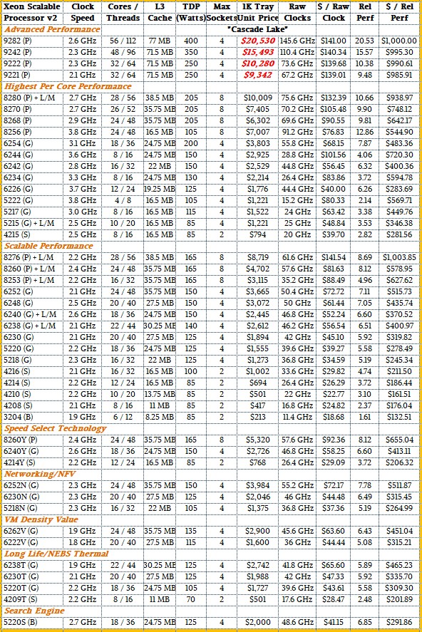
There is a lot in there, and some data that is not. If you want to know which SKUs can support the Apache Pass 3D XPoint memory sticks, which have been given the name Optane Data Center Persistent Memory Modules and which we will call Optane PMMs in contrast to the existing Optane SSDs, it’s easy: The Cascade Lake-AP 9200 series do not support the Optane PMMs. The only Silver Cascade Lake chip that supports Optane PMMs is the Xeon SP-4215. The Bronze Xeon SP-3205 does not support Optane PMMs. All of the other Platinum chips and all of the Gold chips do support Optane PMMs. OK, so maybe that was not really that easy. The Platinum SKUs that support medium (M) and large (L) memory, which is again is 2 TB per socket and 4.5 TB per socket, are designated as such in the table above. The M memory is supported by default on the chips that have it, and the L memory SKUs add another $4,895 to the price shown in the table above and require 512 GB Optane PMMs, which are not yet available, to hit that level.
As you can see from the table, Intel is grouping the Cascade Lake processors into several different groups, each one aimed at a different balance of performance, price, and thermals and as a consequence aimed at a different part of the datacenter. The idea with Cascade Lake was to jiggle the SKUs a bit and put more cores in each SKU and cranked the base clocks a little bit compared to Skylake, Jennifer Huffstetler, vice president in charge of managing data center products and storage at Intel, tells The Next Platform, as well as charging about the same price for the chips, thus yielding a price/performance improvement from generation to generation. This will keep companies buying today’s Xeon SPs when they know Copper Lake and Ice Lake are around the corner. (We will be doing a deeper analysis of this in a follow-up story.)
Although Intel doesn’t say it this way, the plain vanilla Cascade Lake single chip modules are tweaked slightly in two different directions: One emphasizes single thread performance across the cores on each chip – what Intel calls Per-Core Scalable Performance – and the other has somewhat diminished clock speeds and lower thermals as well as lower prices – what Intel calls Scalable Performance. The Advanced Performance multichip module variants do not have list prices, but we have estimated them based on rumors and on the pricing for the plain vanilla; Intel does not want people to do this, but everyone will. There are variants of the Cascade Lake chips aimed at storage (the Y variants), network function virtualization (the N variants), virtual machine density (the V variants), NEBS-compliant for service providers and telcos (the T variants), and even a special SKU for search engines (that lone S variant with 18 cores turboing up to 3.9 GHz in a 125 watt power envelope for a mere $2,000 list price).
The pricing shown in the table above is Intel list price per unit when bought in 1,000 unit trays, as usual, but for some reason Intel is now calling this Recommended Customer Pricing, or RCP. To gauge the performance across the Cascade Lake line, we have did the usual rough approximation by multiplying the cores by the clocks, and to get a sense across Xeon families since the “Nehalem” Xeon 5500s in 2009, which we will do separately, we have adjusted this raw performance upwards for average improvements in instructions per clock (IPC) since the Nehalems launched.
Our touchstone chip against which all others are measured is the four core Xeon E5500 running at 2.53 GHz, which is rated at 1.00. The six core Xeon SP-3204 Bronze has a relative performance of 1.61 by comparison and the top bin Xeon SP-9282 Platinum, which has 56 cores running at 2.6 GHz has a relative performance of 20.53. If you adjust the $744 price of the Nehalem Xeon E5544, it would cost $878, so that is 20.53X the performance, and if our estimate of the price is right for the Xeon SP-9282, it costs 23.4X more to get it. If you want to compare the Xeon SP-8280, that delivers 10.66X the performance, but it costs 11.4X times as much in 2019 dollars to get it. And the Xeon SP-8276 delivers 8.69X the raw oomph, but costs 9.93X more to get it. The top performance bin gets more expensive because it has to.
This is what happens when Moore’s Law is running out of gas. The upside is, look at how much more performance you can cram into a chip, and look at all of the innovative things a modern Xeon SP can do above and beyond the raw integer performance in the arithmetic logic units in the core that we are gauging roughly in these comparisons. These features are what make each successive Xeon generation more valuable, not just the raw integer performance that is table stakes.


Designing Servers In Rapidly Changing Times
When chip makers launch the latest additions of their datacenter processors, server OEMs have historically immediately or soon after followed with a rollout of the latest new or enhanced systems based on those offerings. Then they’d wait until the next big unveiling by another chip maker, and the process starts …
HPE Superdome Flex: The Other Big Iron In The Datacenter
Not every workload can be chunked up and spread across a relatively loosely coupled cluster of cheap X86 server nodes. Some really do much better running on a big, wonking, shared memory system. In the wake of IBM’s announcement of the Power10-based “Denali” Power E1080 three weeks ago, we have …
AMD Rides The High Performance Computing Megacycle
Server buyers have longer memories and perhaps deeper disappointment of AMD’s exit from the X86 server processor business than consumers who buy PCs, and a manufacturing constrained Intel has clearly sacrificed some Core PC chip market share to maintain some Xeon SP server market share over the past two years. …
It’s really nice that they increased memory speed up to 2933 MTps, but personally I was looking for workstation single CPU models with boosted PCIE lanes count.
It would be lovely to see even single SKU with 64-80 lanes ready for multi GPU workstation without PCIE PLX switches and dedicated motherboard similar to ASUS DOMINUS EXTREME with all 4 PCIE fully-fledged x16 ports (as well as ASUS solution to merge 2 PSUs to power beefy CPU and 4 GPUs).
If I were them, I would issue single model (LGA 3647 or even BGA 5903) in which QPI blocks and pins were replaced with PCIE x16 units (leaving behind socket compatybility). It would be perfect for all those GPU accelerated AI/ML workloads.
There’s an error in the tables above – verify the core counts on the 8256…