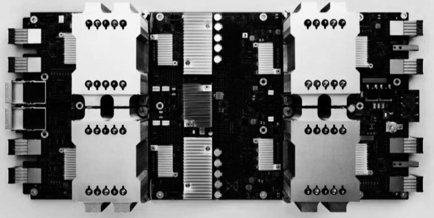
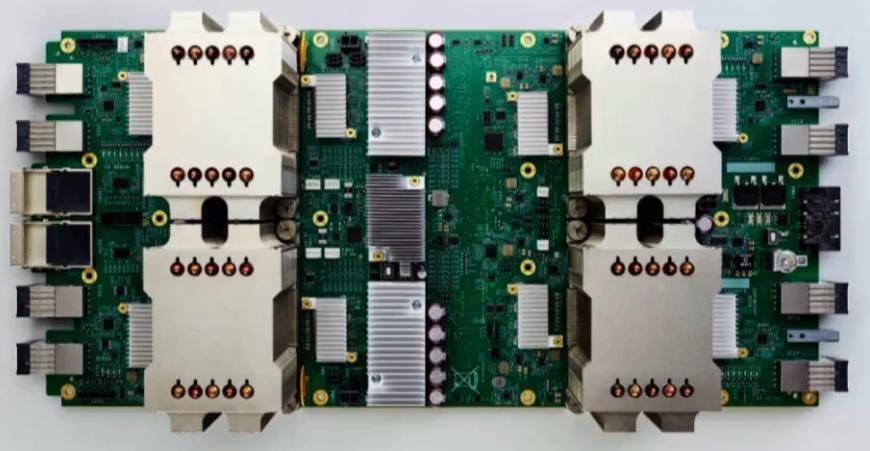
Google laid down its path forward in the machine learning and cloud computing arenas when it first unveiled plans for its tensor processing unit (TPU), an accelerator designed by the hyperscaler to speeding up machine learning workloads that are programmed using its TensorFlow framework.
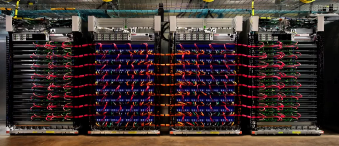
Almost a year ago, at its Google I/O event, the company rolled out the architectural details of its second-generation TPUs – also called the Cloud TPU – for both neural network training and inference, with the custom ASICs providing up to 180 teraflops of floating point performance and 64 GB of High Bandwidth Memory. In addition, the TPU2 boards can be linked together by a fast, dedicated network to create TPU pods, essentially multi-petaflop supercomputers designed for machine learning jobs. As we at The Next Platform have noted before, Google has positioned the TPU2 to accelerate deep learning workloads for consumer-facing workloads, ranging from search and maps to voice recognition and emerging areas like training self-driving vehicles.
However, much of the talk around TPU2 has been just that: talk. Google has outlined the architecture and the strategy behind the powerful ASICs, with the goal of giving researchers and other users another accelerator to join the CPUs from Intel and “Volta” GPU accelerators from Nvidia that populate the Google Cloud and the TensorFlow Research Cloud (TRC). That’s changed. Google is now making the Cloud TPUs available in beta on the Google Cloud Platform for training and running machine model mores quickly, and to make such programs easier to run and available to a wider group of users.
“Traditionally, writing programs for custom ASICs and supercomputers has required deeply specialized expertise,” John Barrus, product manager for Cloud TPUs in the Google Cloud, and Zak Stone, product manager for TensorFlow and Cloud TPUs for the Google Brain Team, wrote in a post on the company blog. “By contrast, you can program Cloud TPUs with high-level TensorFlow APIs, and we have open sourced a set of reference high-performance Cloud TPU model implementations to help you get started right away.”
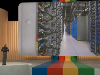
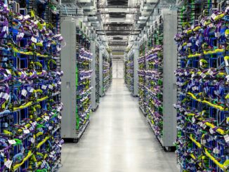
Those reference implementations include such image classification models such as ResNet-50, Transformer for machine translation and language modeling, and RetinaNet for object detection. The Cloud TPUs are available in beta immediately in limited quantities for $6.50 per TPU per hour. The larger TPU pods, pictured below, will become available later this year on the Google Cloud Platform.
Google is touting both the speeds and cost savings users will see when using TPU2 chips for TensorFlow-based workloads, noting that researchers can run their workloads via exclusive access to a network-attached Cloud TPU through a Google Compute Engine virtual machine that they can control and customize, rather than having to wait for their job to be scheduled on a shared compute cluster. Training a machine learning model can be done overnight on a fleet of Cloud TPUs rather than over days or weeks, and using a TPU and a Google tutorial can mean training ResNet-50 to meet the ImageNet benchmark in less than a day for under $200, according to the company. Once the TPU pods are available, ResNet-50 and Transformer training times will drop from almost a day to less than 30 minutes.
In addition, being able to do this on the Google Cloud means not having to invest in the upfront costs of designing and installing a machine learning cluster on-premises or continually having to update and secure the software running across multiple machines in the cluster.
However, it will be interesting to see how much action the internally-designed TPU2 chips get. There’s little doubt that the ASICs will speed up the deep learning workloads in TensorFlow environments, but as we’ve noted, Intel and Nvidia are both continuing to enhance the capabilities of their respective CPUs and GPUs in the area of machine learning and artificial intelligence. When Intel last fall rolled out its 14-nanometer “Skylake” Xeon SP processors – armed with the company’s new Mesh Architecture for faster connections between cores and other processor components – the message was that they were aimed at such emerging workloads as AI, machine learning and virtual reality.
For its part, Nvidia has made such jobs central to its strategy going forward, and last year put the powerful Volta Tesla V100 GPUs onto the market as it looks to maintain the company’s edge running parallel workloads and be the leading accelerator for AI and machine learning tasks. According to Nvidia, the V100 delivers the performance of 100 CPUs, accelerates both neural network training and inference, and provides up to 125 teraflops of performance for deep learning workloads.
Google is positioning the Cloud TPUs as another weapon in its arsenal as it looks to carve into the market shares of cloud computing leaders Amazon Web Services and Microsoft Azure. The goal is to offer Google Cloud customers options for their machine learning workloads that includes a variety of high performance CPUs, including Skylake, and GPUs, like the Tesla V100 accelerator, along with the Cloud TPUs.


will google be able to keep up?
GPUs are already beating them in perf/watt, what happens in 1-2 generations?
Nvidia can keep spending 3 billion USD per generation because there is a market, can google do the same without any serious revenue?
Probably not….
Not even chipzilla could keep chirning oit xeon phis at a loss forever…
Nvidia and Intel are dead in water as far as supplying AI/DL accelerators to hyperscalers is concerned. Google will always prefer TPU to anything else due to power and cost efficiency (it is not all about performance), Amazon is making its own AI accelerators through Annapura Labs and Microsoft while using the Altera/Intel FPGAs will soon have its own ASIC for DL.