

Compute is being embedded in everything, and there is another wave of distributed computing pushing out from the datacenter into all kinds of network, storage, and other kinds of devices that collect and process data in their own right as well as passing it back up to the glass house for final processing and permanent storage.
The computing requirements at the edge are different from the core compute in the datacenter, and it is very convenient indeed that they align nicely with some of the more modest processing needs of network devices, storage clusters, and more modest jobs in the datacenter such as those Web infrastructure loads that run on microservers.
In the past several years, Intel has aimed its Xeon D family at these modest workloads where the workhorse Xeon E5 was overkill. The Xeon D chip, which debuted nearly three years ago, was the company’s first 14 nanometer part and the first in the “Broadwell” line of processors. This Broadwell Xeon D-1500 series was also Intel’s first pass at trying to create a Xeon system on chip (SoC) that could compete with the fully integrated designs of the several Arm server chip makers who were trying to get their foot into the datacenter door with an oblique attack rather than a direct assault on the workhorse Xeon E5 processors that dominated core compute back then and still do today. It was famously adopted by Facebook in its “Yosemite” microserver, which is an integral part of its server and storage infrastructure because sometimes having a lot of modestly powerful cores is better than having fewer beefier ones.
Intel had a three pronged approach to blunt the attack of the Arm collective. At the low end was the Atom series, which includes the 22 nanometer “Avoton” C2000, launched in September 2013, sporting up to eight “Silvermont” cores. This was followed up by the “Denverton” C3000 chips, launched last August with up to 16 of the “Airmont” Atom cores on the die. Sitting adjacent to them is the Xeon E3 family of chips for single-socket server and workstations, which were updated with the “Skylake” cores way back in June 2016 and which were updated with the “Kaby Lake” cores in April 2017. It is not clear if there is a roadmap going forward for these Atom or Xeon E3 server chips, and Jason Kennedy, director of product marketing for datacenter platforms at Intel, did not want to talk about the future of these two lines when we chatted with him about the shiny new Skylake Xeon D chips coming out today, which are called the Xeon D-2100 series.
The Xeon D update is important not so much because there will be tens of millions of units of these devices shipped in the world, like the regular Xeon E5 and Xeon SP chips. That is not going to happen. We reckon that the number of Xeon Ds that will ship in a year is probably around two orders of magnitude lower than that – call it hundreds of thousands of units, generating hundreds of millions of dollars in revenues. Keeping that money out of the hands of competitors is important because Intel also has to protecting its core datacenter processor business against insurgents from the Arm collective as well as against a resurging AMD with its Epyc X86 server chips and IBM with its beefy Power9s. If the Arm collective attached from below and from the flank, and gets success, that will fuel their attack on the core datacenter, which they also want to do. The Skylake Xeon D is designed to cover the gap between the Xeon SP, which is really not aimed at single socket servers, and the Atom C3000, which doesn’t have enough oomph for certain kinds of work, particularly when floating math is involved. The Xeon D has been successful in keeping the competition at bay, but the competition is getting better, and that means Intel has to up its game.
That means moving to the Skylake core and the on-chip 2D mesh interconnect that debuted with the Skylake architecture. The Xeon D-2100 also has the new L2 and L3 cache hierarchy of the Skylake Xeon SPs, and they do not drop L3 cache from the memory stack as the Atom C2000 and C3000 chips do. So, in effect, the Skylake Xeon D is kind if a cross between a Skylake Xeon SP and an Atom C3000, leaning a little more toward the Xeon and a little less towards the Atom.
It is interesting that the Xeon D-2100 did not move to a future Xeon core like “Cannonlake” and an even more energy efficient 10 nanometer process, which we are certain that Intel would have wanted to do with this iteration of the Xeon D if it had a chance. This is what it did with the original Xeon D, using it to work the kinks out of the 14 nanometer wafer etching process and getting some server margins at the same time. It is looking like the move to 10 nanometers is tougher than expected, just like the 14 nanometer ramp was tougher and has pretty much resulted in moving away from the tick-tock method Intel had used for so long to great success.
Below is the block diagram of the Skylake Xeon D:
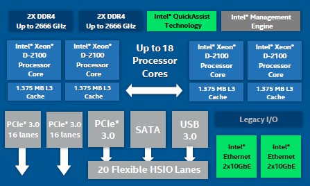
This is more of a conceptual block diagram than is usual from Intel, and it might give the mistaken impression that the Skylake Xeon D was a monolithic chip with all of its components on board. This is not the case, just as it was not with the original Xeon D, and in fact the I/O south bridge – what Intel calls the PCH – is actually a separate chip that is embedded on the Xeon D package and connected to the CPU thorough high speed direct memory interface (DMI) links. Kennedy did not divulge the specifics, but we are pretty sure that the Xeon D-2100 includes an integrated “Lewisburg” C620 series PCH chipset, based on the feeds and speeds of the I/O handing off the package. The scale of the Ethernet controllers and the throughput of the QuickAssist encryption engines certainly matches that of the C625, C626, C627, and C628 chipsets.
The Xeon D-2100 has up to 18 cores on the die, with each core having its own 1.375 MB L3 cache segment affiliated with it. Each Skylake core has 32 KB of L1 instruction cache, 32 KB of L1 data cache, and 1 MB of L2 cache tied to it that sit between the cores and that L3 cache. The L3 cache is non-inclusive, you will remember, which means that the L2 cache lines may not be in the share L3 cache. The L2 cache is bigger and the L3 cache is smaller with this Xeon D than compared to the prior Xeon D.
The Skylake Xeon D chips range in clock speed between 1.6 GHz and 2.2 GHz at their base, and can crank up to as higher speeds depending on how many cores are activated and how many are in a low power state using Turbo Boost 2.0 overclocking. The initial charts from Intel suggested that all cores could crank to 3 GHz, no matter what, and we though this was very exciting, but the laws of physics prevailed and this typo was fixed. (Sorry to be a downer, everyone.) With only two cores fired up on any of the SKUs, you can hit that 3 GHz, and with three or four cores you are at 2.8 GHz and it drops down by 100 MHz for every couple of cores from there to the base frequencies and full cores on.
The Xeon D-2100 chip has two DDR4 memory controllers, each with a pair of channels, and memory can run at 2.13 GHz, 2.4 GHz, or 2.67 GHz, depending on the models. Using 128 GB memory sticks, you can crank up the capacity as high as 512 GB, which is pretty big for a lot of networking, storage, edge, and microserver workloads. We think 64 GB or 128 GB will be far more common, given the cost of main memory these days.
All of the new Xeon D chips have two static PCI-Express 3.0 controllers with 16 lanes, and all but one of the chips – the top bin D-2191 – have four integrated 10 Gb/sec Ethernet network interfaces (a pair of two port controllers) coming off the package. (It is not clear why a server SKU does not have integrated networking.) The Ethernet controllers support RDMA (which we suspect is iWARP not RoCE), which is vital for storage and HPC workloads, and increasingly, for other kinds of jobs such as machine learning.
All of the chips have 20 lanes of I/O coming off the Lewisburg PCH, which Intel labels as High Speed Input/Output, or HSIO, and says implies is configurable as PCI-Express 3.0, SATA storage, or USB 3.0 ports. To be precise, up to 20 of the lanes can be PCI-Express, up to 14 can be SATA, and up to four can be USB.
The whole shebang fits into a Socket FCBGA that is 45 millimeters by 52.5 millimeters.
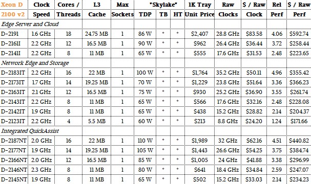
Here is the SKU stack for the Xeon D-2100 v2 chips:
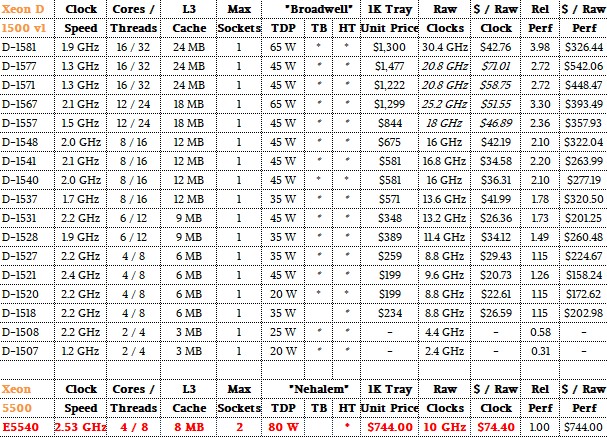
And here are the Xeon D-1500 v1 chips with the baseline “Nehalem” Xeon E5540 that we use to gauge relative performance across the Xeon line:
Now, let’s start with some observations, and it is here that we can once again talk about the Skylake being a premium product, with lots more features, at a premium price, as we did with the Xeon SP compared to the prior six generations of Xeon server chips last year.
Depending on how you compare the chips across the two Xeon D lines, the price/performance of the devices, at least at the list prices that Intel gives out for 1,000-unit trays, has not really improved. In some cases, the new Xeon D-2100 series are actually more expensive when gauged against the rough relative performance on integer workloads, as we do in the above chart. Just a reminder: Relative performance is the number of cores times the clock speed times the instruction per clock (IPC) improvements that Intel has attained with each successive core change since the Nehalem architecture that came out in march 2009. For fun, we also have just the raw aggregate clocks in the tables above, but we think our relative performance metric is more useful since it allows a comparison across Xeon generations as well as within them.
Speaking very generally, on the performance per watt front, the new Xeon D-2100s are not better than the Xeon D-1500s, and that is because the wattages have crept up as other features have been added to the cores, such as QuickAssist encryption and AVX-512 floating point math units. It is these features that are now required for network, storage, edge, and microserver workloads, and Intel is charging a premium for them. Had there been a process shrink to 10 nanometers, instead of sticking to 14 nanometer processes, Intel might have been able to lower the wattage, add a few cores, and even drop the price a bit. But that is not what happened because Moore’s Law is not moving smoothly even if it does stay on track, as Intel contends. But this is happening more because of tricks in design, not straight transistor shrinking anyway, so the point is moot. Normal scaling has slowed, and we don’t have 10 nanometers for Skylake, and that means adding features costs more than it might have otherwise. And with the X86 architecture reigning supreme and the Arm competition not coming full bore yet and AMD and IBM focusing on core compute, Intel can and is charging a premium for these features.
All of the chips have AVX-512 units, but as is the case on some of the lower bin Xeon SP parts announced last July, the second fused multiply add (FMA) unit in the Xeon D-2100 is not activated. That means it does 32 single precision or 16 double precision floating point operations per clock, half that of the full-on Xeon SP processors. This is the same raw performance as the Broadwell core in the Xeon D-1500, but the amount of clock cycles it takes to do operations and the way they get done is very different, resulting in performance improvements not shown in the peak numbers. The AVX-512 units, says Kennedy, help with faster data transfers and faster encryption and are not just used for raw floating point.
The QuickAssist encryption and decryption accelerator, unlike the AVX-512 floating point unit, is not activated on all of the Xeon D-2100 chips. In fact, there are only five SKUs that have them. The D-2187NT and D-2177NT parts can run QuickAssist at 100 Gb/sec, the D-2166NT and D-2146NT parts can run it at 40 Gb/sec, and the D-2145NT can run it at 20 Gb/sec. The higher SKUs support faster DDR4 memory as well as faster QuickAssist throughput, and there is definitely a high premium for these capacities. In general, the Xeon D-2100 chips that support faster memory cost more, and that shows that Intel is focusing on throughput and latency, like its customers are, and reckons it can charge more for that. It will be interesting to see if the Arm collective that is also chasing networking, storage, edge, and microserver workloads will also do the same, or if they will do what AMD is doing with the Epyc chips and just turn everything on full bore to attract customers with a simpler SKU stack and aggressive pricing.
Intel is touting the fact that the Xeon D-2100s support four times more main memory than the Xeon D-1500s, and that is a function of doubling up the main memory controllers from two to four and doubling the capacity on the DIMMs. The Xeon D-2100 has four memory controllers, with two DIMMs per channel, and can support 64 GB memory sticks. In theory, Intel could support 128 GB memory sticks from the 32 GB memory sticks in the original Xeon D, and push capacity up to 1 TB per socket. It would be very funny to see someone put eight 128 GB sticks in a microserver, at around $5,000 to $6,000 a stick. . . .
On compute workloads, in this case running an NGINX Web server with encryption turned on, a Xeon D-2187NT with 16 cores running at 2 GHz and the full bore QuickAssist is delivering 2.9X the performance of a Xeon D-1553N, which has eight cores running at 2.3 GHz. This is much better than the 1.6X performance improvement on the SPECint_rate2017 integer test pitting the Xeon D-2183IT variant, which has 16 cores running at 2.2 GHz, against a Xeon D-1581, which has 16 cores running at 1.9 GHz. On warm storage workloads, which have cryptographic hashing to spread their data around a cluster, a Xeon D-2183IT, which has 16 cores running at 2.2 GHz, does about 2.8X the work of a prior Xeon D-1587, which has 16 cores running at 1.7 GHz. And running the Data Plane Development Kit for virtualized networking, the Xeon D-2183IT can beat the D-1553N by about 29 percent on packet forwarding as gauged by the data rate out of L3 cache and into the network.


Intel Aims For Zettaflops By 2027, Pushes Aurora Above 2 Exaflops
Just because Intel is no longer interested in being a prime contractor on the largest supercomputing deals in the United States and Europe — China and Japan are drawing their own roadmaps and building their own architectures — does not mean that Intel does not have aspirations in HPC and …
Intel To Amp Up Security With “Ice Lake” Xeon SP Servers
Security is one of those necessary things that should not be an afterthought, but often is, and ideally is so invisible that it doesn’t get in the way of applications and the infrastructure it runs on. Speaking very generally, the cost of security has been so high on servers that …

Pandemic Compute Needs Drive Intel’s Data Center Group
The first half of last year was relatively weak for Intel’s Data Center Group last year, but despite the coronavirus pandemic – and in some cases, we think because of it – the world’s largest datacenter chip manufacturer is looking to not only have a good first quarter, as it …
Be the first to comment