
Increasing parallelism is the only way to get more work out of a system. Architecting for that parallelism required requires a lot of rethinking of each and every component in a system to make everything hum along as efficiently as possible.
There are lots of ways to skin the parallelism cats and squeeze more performance and less energy out of the system, and for DRAM memory, just stacking things up helps, but according to some research done at Stanford University, the University of Texas, and GPU maker Nvidia, there is another way to boost performance and lower energy consumption. The new subchannel DRAM architecture was developed in part from funding from the Department of Energy and the Defense Advanced Research Projects Agency in the United States as well as from Nvidia, and the ideas embodied in this new subchannel architecture were tested out on a simulated “Pascal” P100 GPU compute engine.
The subchannel architecture was detailed in a paper called Architecting An Energy-Efficient DRAM System For GPUs, which was presented back at the recent High Performance Computer Architecture symposium hosted by the IEEE. Researchers Bill Dally and Stephen Keckler of Stanford and Mike O’Connor of the University of Texas worked together on the subchannel architecture along with Niladrish Chatterjee, Donghyuk Lee, Daniel R. Johnson, and Minsoo Rhu of Nvidia. (Dally, of course, does double duty and is also chief scientist at Nvidia.) Interestingly, it looks like this new subchannel architecture could not only improve the energy efficiency of regular DRAM DIMMs but also could, to our eye anyway, also be used to improve the energy efficiency of the 3D stacked memory that would appear to be integral to future exascale-class systems, including the High Bandwidth Memory (HBM) employed by Nvidia, AMD, and Fujitsu in their various parallel compute engines.
As the paper explains, a massively parallel compute engine, whether it is a GPU or a parallel X86 device, is going to need lots of bandwidth. Nvidia itself was shooting for 1 TB/sec with the HBM2 stacked memory with the Pascal P100 GPUs, but peaked at 720 GB/sec. That is still far better than the 288 GB/sec offered by the GDDR5 frame buffer memories on the top-end “Kepler” and “Maxwell” generations of GPUs from Nvidia, but the researchers say that it will take at least 4 TB/sec to create a balanced exascale system, but to do so in a flat power envelope is a serious challenge, and perhaps it is the challenge for exascale computing, far more difficult than cramming a lot of cores in a socket and across nodes and racks and rows. The memory stacking techniques employed by HBM (and its rival Hybrid Memory Cube method from Micron Technology and Intel) cut the energy required to pass bits between the CPUs and DRAM by radically shortening the wires between these two circuits and widening the paths between them. But 3D stacking doesn’t do anything to reduce the energy consumption required to move the data from the memory cells in the DRAM chips out to the I/O interface on that DRAM and into the processing complex. This, in a nutshell, is what the subchannel architecture proposed by these researchers is all about tweaking, and it deals with the fact that for many applications running on GPUs, data locality between channels linking to CPUs and the DRAM cells on DIMMs or in HBM modules is not particularly high, and this burns up a lot of energy.
The DRAM subsystem has two key energy components. The row energy is the amount of juice needed to precharge a bank of memory and activate a row of cells and the column energy is the juice needed to access a subset of the data on that activated row and move it out to the pins in the I/O channels so it can be send to the CPU. How energy efficient the row and column activations are depends on the locality and the architecture, as this chart using GPU data shows:
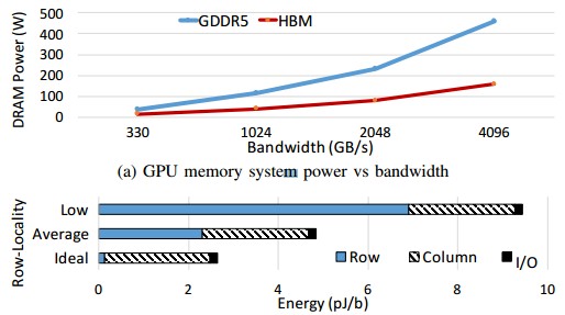
As you can see, the energy for the column accesses and for the I/O pins does not change very much depending on the locality of the data in the DRAM and the channel it is requested from, but this is absolutely not the case with the row activations. When the locality is good – the right channels are closest to the memory – then this row energy is very low, but when the locality is poor, it balloons and overwhelms the other factors. Clearly, then, it is necessary to improve the locality of data accesses, and that is done in this subchannel memory architecture by partitioning the memory chunks and allowing more granular access to them.
“First, several GPU applications have intrinsically low locality,” the researchers explain in the paper. “Applications that often perform data dependent memory accesses (pointer chasing) or sparse, irregular accesses to a data structure (bfs, bh, dmr, mst, sp, sssp, MCB and MiniAMR) naturally have low spatial correlation between successive accesses. GUPS, which is designed to randomly access memory, is the most extreme example of this behavior. All of these applications access one or two DRAM atoms (32B each) per activate. Second, even when applications tend to access dense data structures, there is limited row-buffer locality due to interference between the large number of simultaneously executing threads.”
As an example, take the Pascal P100 GPU. It has 122,880 threads across the full complement of 60 Streaming Multiprocessors (SMs), which access data across 32 HBM2 channels, each with 16 banks. So on average, 240 threads on the GPU are contending for the single row-buffer in each bank. As a consequence, the researchers say, even with deep memory controller queues and aggressive request reordering to harvest row locality, GPUs suffer from frequent bank conflicts. This is particularly true of compute workloads running on GPUs, which have less locality than graphics workloads.
This proposed subchannel architecture also has a data reordering mechanism that boosts efficiency for the column accesses as data moves from fat internal buses of the DRAM out to the skinnier buses embodied in the I/O pins.
Here are the feeds and speeds of the test Pascal Tesla P100 card that the team ran their simulations on:
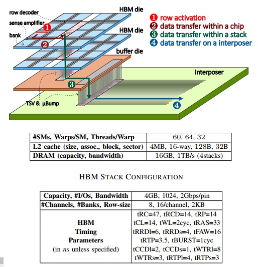
This looks like a perfectly normal P100 card, with the exception that it has 1 TB/sec of bandwidth instead of the 720 GB/sec of the actual P100. It has the same four layers of stacked DRAM, and all the same basic feeds and speeds. The memory controller in this hypothetical Tesla P100 complex is optimized to harvest maximum bandwidth, according to the researchers, has optimized address mapping, deep request buffers, aggressive request reordering, and batched write-drains to minimize write-to-read turnarounds, and its caches use a 32B sector size for higher performance and energy-efficiency.
Add it all up and these architectural changes increase the efficiency of DRAM memory by 35 percent, according to the researchers, and the resulting system, using an emulated Pascal and DRAM memory complex, has an average of 13 percent better performance to boot. Some of the tests run by the researchers had a much higher performance gain from the subchannel architecture, particularly those that are bandwidth sensitive, which saw gains of 35 percent to 152 percent. And all of this by only adding 2.6 percent to the area of the DRAM chips to accommodate the subchannel circuitry.
The question we have is what effect this subchannel architecture might have on plain old DRAM DIMMs. Such dramatic performance boosts and energy efficiency gains would be a good thing for regular servers to have, too. And it would be nice to have it on other compute complexes like Intel Xeon and Xeon Phi, AMD Opteron and Radeon, and IBM Power9 compute as well.

Nvidia Rounds Out “Ampere” Lineup With Two New Accelerators
In a world where GPUs have tens of billions of transistors and chip manufacturing techniques are costly and yields are particularly tough because of the largesse of these devices, every chip that comes of out the foundry is sacred. That’s why chip companies have diverse SKU stacks for their devices. …
Groq Says It Can Deploy 1 Million AI Inference Chips In Two Years
If you are looking for an alternative to Nvidia GPUs for AI inference – and who isn’t these days with generative AI being the hottest thing since a volcanic eruption – then you might want to give Groq a call. It is ramping up production on its Language Processing Units, …
Microsoft Azure Blazes The Disaggregated Memory Trail With zNUMA
Dynamic allocation of resources inside of a system, within a cluster, and across clusters is a bin-packing nightmare for hyperscalers and cloud builders. No two workloads need the same ratios of compute, memory, storage, and network, and yet these service providers need to present the illusion of configuration flexibility and …
“This proposed subchannel architecture also has a data reordering mechanism that boosts efficiency for the column accesses as data moves from fat internal buses of the DRAM out to the skinnier buses embodied in the I/O pins.”
How does this differ from the JEDEC HBM/HBM2 standard with its 8, 128 bit channels, structure? So aren’t the majority of DIMM Based DRAM channels 128 bits to begin with? AMD’s and SK Hynix’s now JEDEC HBM/HMM2 standard has those smaller 128 bit channels intrinsic to the JEDEC HBM/HBM2 standard.
” Nvidia itself was shooting for 1 TB/sec with the HBM2 stacked memory with the Pascal P100 GPUs,”
The JEDEC standard deals with only what it takes to make a single stack of HBM/HBM2 so that maximum bandwidth is a factor on how many HBM/HBM2 stacks are used and the chosen bandwidth with a single stack of HBM2 supporting up to 256GB/s bandwidth. There is probably the option of clocking lower any HBM2 stacks to save on power at the cost of total effective bandwidth.
And really what is the job of the base die in the JEDEC HBM2 standard, is that where there is room to make any custom decisions with regards to splitting of the sub-channels on any HBM2 DRAM die stacks to better match GPU loads, and is that more a concern for Samsung, and SK Hynix/other HBM makers for their respective GPU/Other clients and JEDEC/Members itself. Is this something that can be done in a hardware abstracted manner while still adhering to the JEDEC standard.
“How does this differ from the JEDEC HBM/HBM2 standard with its 8, 128 bit channels, structure? So aren’t the majority of DIMM Based DRAM channels 128 bits to begin with? AMD’s and SK Hynix’s now JEDEC HBM/HMM2 standard has those smaller 128 bit channels intrinsic to the JEDEC HBM/HBM2 standard.”
HBM addresses the I/O energy it takes to transfer data from the DRAM to the host processor. This proposal tries to address the energy it takes to move data from the DRAM bit cells to the I/O interface within the DRAM. It makes some changes to the hierarchy of access signals within the DRAM. It allows for finer control of activation commands so there are less unneeded activations in cases of low data locality, a condition they say is common in GPU compute applications.
It does not replace what HBM achieves, but rather can be used along with it. It really does not have anything to do with HBM per say, it’s simply an optimization of DRAM for GPUs that looks like it can be used in conjunction with HBM or GDDR.