

Depending on how you want to look at it, the half dozen companies that have aspired to bring ARM architecture to the datacenter through chips designed specifically to run server workloads are either very late to market or very early. The opportunity to take on Intel was arguably many years ago, when the world’s largest chip maker was weaker, and yet despite all of the excitement and hype, no one could get an ARM chip into the field that clearly and cleanly competed against Intel’s Xeons and did so publicly with design wins that generated real volumes that took a bite out of Intel’s business.
Qualcomm, which makes its billions selling chips for smartphones, tablets, and wireless networks, wants to be the first, and it may fall to Qualcomm to actually make ARM servers a commercial product because the other players in the market that have tried are not yet succeeding. Broadcom, the networking giant that is the result of the $37 billion merger between Avago Technologies and the prior iteration of Broadcom in May 2015, was perhaps the best hope of a giant bringing a volume-class ARM server product to the field, but we have heard persistent rumors since ARM TechCon a month ago that Broadcom has ceased development of its “Vulcan” homegrown ARM server chips. After that merger between Avago and Broadcom, the new Broadcom was roughly half the size of Qualcomm and a quarter the size of Intel, just too give you a sense of scale, which is vital when it comes to chip manufacturing. Broadcom has refused to confirm or deny the rumors about Vulcan being canceled, talk that really started as soon as Avago bought Broadcom, which announced its intent to enter the server fray in 2014 and which was expected to get chips in the field in 2015.
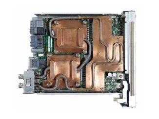
Anand Chandrasekher, senior vice president and general manager at Qualcomm Datacenter Technologies, who is spearheading the development of the “Amberwing” Centriq ARM server chips, is undaunted by the failure of Calxeda, Samsung deciding to not do server chips, and maybe Broadcom, AMD, and possibly Applied Micro pulling back, too. Because of the intense competition between Intel and the rest of the chip world, the dominant supplier of chips for smartphones and wireless networks has been secretive about its homegrown ARM server chip core, which ironically is called “Falkor” after the good luck dragon in The Neverending Story. And Chandrasekher did not revealing much when he divulged some details about the Amberwing chip, either, as the company has started shipping samples of its second server-class chip to early customers.
In October 2015, Qualcomm showed off a prototype generation of ARM server chips, based on an earlier iteration of the Falkor core, which is a custom ARMv8 design and which is not just a cookie-cuttered variant of the “Kryo” cores used in the Snapdragon line of chips that The Q sells for clients and networking devices. This prototype ARM server chip, whose name was not revealed, is limited to a single processor socket per machine, and for many workloads, particularly at hyperscalers, that is fine so long as that socket has enough oomph and memory. But Qualcomm has admitted to The Next Platform that Qualcomm and its early adopter customers do anticipate needing for SMP or NUMA clustering to glue ARM chips into a shared memory system with more oomph; we suspect that the Centriq line of Qualcomm ARM server chips will span two sockets at least, and possibly more.
In February this year, when Qualcomm was talking about its broader business with Wall Street, we analyzed everything it said about the server chip business and guessed that the 24-core prototype ARM chip from the company was implemented in a 14 FinFET nanometer process, just like the Snapdragon 820 is, although we conceded that it could be fabbed by Taiwan Semiconductor Manufacturing Corp instead of Samsung Electronics. The caches, clock speed, accelerators, NUMA or SMP scaling, memory capacity, and other important aspects of the prototype Centriq ARM server chip were not divulged.
That chip doesn’t really matter, except to demonstrate the custom ARMv8 core design to potential hyperscaler customers, and Qualcomm has previously confirmed to The Next Platform that it is working with all of the eight key hyperscalers (chant them along with us, Google, Amazon, Facebook, Microsoft, Baidu, Tencent, Alibaba, and China Mobile) in one form or another on the Centriq project – a good reason for Broadcom, which has other fish to fry, to back out. We have heard that one of the big hyperscalers in Silicon Valley – there are only two – are behind Qualcomm’s move into server chips. Our guess is Google is the one pushing hard.
Earlier this year, when Qualcomm was ramping up it ARM server chip PR campaign, the company said that it would be using the latest FinFET process node to make the Amberwing chips. That statement was vague enough to give Qualcomm some wiggle room and sow some confusion and keep Intel and everyone else guessing. TSMC and Samsung were aiming to get 10 nanometer manufacturing processes up and running in production by the end of 2016, and we guessed if Qualcomm was hoping to get a part with 48, 64, or 96 cores out the door, it no doubt wants to be on these 10 nanometer processes. The number of cores always depends on how brawny they are, and considering the customers are hyperscalers, these cores would have to provide about the same performance as a Xeon thread to be interesting. Our wild guess was that if Qualcomm can do 24 cores in a prototype in 14 nanometer FinFET processes, then it can possibly get 32 cores or 36 cores in a 10 nanometer process with fairly brawny cores and maybe 48 cores or 64 cores if they are a bit wimpier.
As it turns out, Chandrasekher confirmed to The Next Platform that the Amberwing chip will be called the Centriq 2400 line, with variations in core counts, cache sizes, and clock speeds as you would expect, and that it would top out at 48 cores and be implemented in the latest 10 nanometer processes like the latest-greatest Snapdragon 835 chips, which were unveiled two weeks ago, are. These Snapdragon 835 chips will ship in the first half of 2017, and the 48-core Amberwing Centriq 2400 chips.
We asked Chandrasekher who was the foundry for the Centriq 2400 chips, and he did not reveal who it was, but when we suggested it could be Intel, his former employer who is working on 10 nanometer processes, he nearly choked on his tea laughing and confirmed that it, indeed, was not Intel that is making Qualcomm’s chips. (Hey, that’s how Intel started down its $16.7 billion road to buying Altera. First comes foundry, then comes acquisition, then comes integration in the Xeon package. . . .)
While the design of the Amberwing chip will be interesting, the process node and cadence between mobile and server chips is perhaps more revealing about Qualcomm’s plan and its prospects for success in ARM server chips where others have either failed or not exactly set the bit barns on fire. The adoption of 10 nanometer processes for Amberwing puts this chip at roughly the same launch schedule as Intel’s future 28-core “Skylake” Xeon E5 v5 processors, which are expected in the middle of 2017. (We are hearing about a July launch from server OEMs.) But Intel is only on 14 nanometer processes for Skylake Xeons, and won’t get 10 nanometer chips into the field until maybe 2019 with “Cannonlake” Xeons if there is an interim 14 nanometer “Kaby Lake” Xeon in 2018, as we expect. The gap between a design and process between PCs and servers for Intel has widened to about 23 months or so, and Qualcomm is going to cut that gap to somewhere less than a year between the Snapdragon and Centriq.
The natural thing to wonder is how much commonality there is between Snapdragon and Centriq. “Some things carry over, but a lot does not,” Chandrasekher tells The Next Platform. “The core is a dedicated server core, and the system on a chip is also dedicated to servers as well. Those two things are the bulk of the investment, and we are on a leading edge node. So when you compound all of those, it is not a trivial undertaking from a development cost standpoint.”
Being out first is a key factor in Qualcomm’s strategy, and it is in stark contrast to the hang-back attitude that AMD, Applied Micro, Cavium, and Calxeda have had with their ARM server chip efforts. While Chandrasekher said that Qualcomm was committed to keeping the gap small between mobile chips and server chips and on being first on process nodes for server chips, he said there was no chance that The Q could get server chips out ahead on any given process, as FPGA makers sometimes are able to do. The size of the server chips requires for the yields to be improved using volume mobile chips, and their volumes are so much higher than for FPGAs. The numbers do not work.
We had a very long conversation about the chip business and servers with Chandrasekher, and we will be following up with that shortly. It was interesting and fun. But here’s a teaser:
“We are accelerating innovation in the datacenter,” says Chandrasekher. “That is our goal, and part of that is being first in the market on leading edge nodes, and part of that is being able to take advantage of the SoC skills and competencies that Qualcomm already has so we can integrate a lot. And then we have cadence. We think the market is crying for this kind of accelerated innovation. If we execute – and at the end of the day, strategy is just strategy, and we have to execute – I think the market will be quite welcoming.”
While two would be better, the world only needs one good, strong ARM server chip vendor to be successful.

HPC Pioneers Pave The Way For A Flood Of Arm Supercomputers
Over the past few years, the Arm architecture has made steady gains, particularly among the hyperscalers and cloud builders. But in the HPC community, Arm remains under-represented. But perhaps not for long. The “Fugaku” system at RIKEN Lab in Japan is without a doubt the largest and best known Arm …
Making Dollars And Sense Of Arm Holdings
The only thing stronger than having absolute control, as happens in monopolies and oligopolies, is the strength that comes from numbers. Both are economic principles as well as technical ones, and they both come together powerfully in the IT sector in general and in the semiconductor industry specifically. In this …
Designing Chips With The Cloud And Edge In Mind
Renee James knows about processors and she knows about the cloud. In a career at Intel that spanned more than 28 years and saw her rise to become president of the chip giant, she also ran a range of divisions within the company, including HPC, software and the cloud. She …
Guys, guys you can’t just simply compare different Foundry nodes as there is a lot of misinformation and marketing nonsense involved. For example 14nm of Samsung is not as dense as 14nm on Intel. So comparing these numbers is idiotic. The predicted 10nm of Samsung and of TSMC is just about slightly below Intel’s 14nm at the moment. (So not really true 10nm) So there is not much of a process lead at all.
But it will be interesting to finally see how a beefed up ARM-design chips will stack up in the performance/watt department. My rough guess is that there will not be much of a difference to a x86 one.
Intel is leading in HD SRAM cells but HP SRAM or “regular” logic densities are questionable.
And point is that HD SRAMs are too slow (useles in production chips), so in real life foundry 14/16nm achieves aprox. double density compared to Intel’s mighty process.
So all on this case was just another Intel’s way, how to cheat in benchmarks. Because Intel love cheating.
Aren’t you talking about TSMC? TSMC has only published HD SRAM for 7nm, and I challenge you to find HP SRAM for their 16nm. Intel on the other hand always quotes HP SRAM, which for 14nm is 0.0588um^2. Please tell me where you can find a cell with half that size. In the meantime I will conclude your post is FUD.
Yada yada witeken, you are well known Intel TROLL and what Intel wrote is bible for you, even when TSMC publicly said something different. So there is no point to discuss with you.
Do you have any proof to back any of your outrageous claims?
As I do:
https://www.semiwiki.com/forum/content/6160-2016-leading-edge-semiconductor-landscape.html
PDK’s are not publicly available, you have to get them yourself. I hope we will see more on this topic after more of Intel’s PDK’s become publicly available (which will happen if they did not lied that they are now foundry for LG).
For now, you can look at existing silicon. P100 has 15B transistors (6 TFlops). Intel’s equvalent to this, KNL, is supposed to have twice the transistors count (30B) and consequent double performance. But it only has half of the transistor count (slightly more than half thanks to bigger die area).
Or you can compare processors (SPARC M7). Or you should wait for 14nm ZEN/POWER 9.
Probably someone lied again.
I know this is not exact measurement, but when you look at specific rules (or power limitations for example) at PDK then it became clear.
You are comparing Oranges with Apples again. P100 is a complete different design to KNL you don’t know anything about how much die area is used for what purposes.
You would have to do the exact design to compare two fab processes which is already nearly impossible as everybody in the industry knows if you switch from one fab to another you have to use different tools and there are different design restrictions.
Your first post was still of good quality (“Guys, guys you can’t just simply compare different Foundry nodes as there is a lot of misinformation and marketing nonsense involved.”), but then you link to a site that itself publishes loads of misinformation and marketing nonsense.
Your post does not qualify as proof in any scientific sense.
I would say ASML knows a lot more than you people who claim to know things at least they are in the business of semi conductor manufacturing and what exactly are your credentials?
Why would there be a Kaby Lake Xeon as this article suggests? The architecture of KBL is the same as SKL. And SKL-EP will already be made on the 14nm+ process node.
The only reason why Intel would want to wait for CNL-EP is because of the yield on these big chips.
So I think there’s a reasonable chance Intel will release Cannonlake Xeon-D in 2018 to go up against these Qualcomm server chips. (Or their Atom microservers? Haven’t heard anything about those in a long while.)
Will it support SVE? Can we expect overshoted peak performance? (like 64 or 128 Flops per cycle)
I’m loving this. With Windows 10 soon to support ARM chips too (for x86 apps), and big data center companies finally being ready to embrace decent ARM chips, I feel like this is the moment when ARM (chip makers) actually begins the disruption of Intel.
With AMD Zen coming as well, things are going to get rough for Intel very soon. However, I fear AMD may not be able to win back a whole lot of market share from Intel, because by the time that happens, ARM chips will have taken a significant portion of the market.
But this could mean that perhaps in a few years, Qualcomm will be rich enough from its newly found PC and data center revenues to buy AMD. Then the will will REALLY begin, with Qualcomm going 1 on 1 against Intel in PCs, servers, machine learning, and even super computers. I can’t wait. That sort of competition will help accelerate progress in a lot of areas.
Agree this could spell really bad news for Power and AMD, as they will be caught between a rock and a hard place.
If that’s a custom ARMv8A running micro-architecture based Qualcomm chip that is engineered to run the ARMv8A ISA then windows 10/legacy bloat is currently only optimized to run on that exact custom Qualcomm SKU! And What are the exact differences between the Qualcomm ARMv8A ISA running custom micro-architecture and ARM Holdings reference ARMv8A running reference micro-architectures.
If the Qualcomm chip’s underlying hardware has a larger reorder buffer and a slightly different cache subsystem and such other internal differences then Qualcomm will have had to supply Microsoft’s software engineers with that exact chip’s optimization manuals so that they can produce an optimizing compiler/s that takes into account the Qualcomm CPU’s exact internal idiosyncratic execution and decoding engine differences and other internal CPU hardware subsystems differences.
Intel’s brand of x86 32/64 bit ISA running hardware is different at the micro-code and caching, decoding levels in Intel’s hardware that executes the x86 32/64 bit ISA than AMD’s respective x86 32/64 bit ISA running hardware under AMD’s respective underlying hardware features. So Intel’s assembly language optimization manuals are going to be different than AMD’s assembly language optimization manuals. And the Compiler System Software engineers will have to have the respective CPU makers’ optimization manuals to tune the compiler’s optimization passes to produce compiled code that does not produce excessive cache thrashing or other ill effects in the underlying hardware of any custom CPU micro-architecture that is engineered to run the x86 32/64 bit ISA. The same is true for any custom ARMv8A running micro-architectures.
It’s entirely possible to run one makers x86 ISA based compiled code on another maker’s processor that is engineered to run the same x86 ISA, but that code will not run in an optimized state. Ditto for any custom ARMv8A ISA running custom micro-architectures from those top tier ARM holdings architectural licensees who only license the ARMv8A ISA from ARM Holdings. These top tier architectural licensees engineer their own custom micro-architectures that can execute the ARMv8A ISA! So each of their custom ARM CPU cores requires its own optimization manuals and Optimizing compilers that are tuned to produce optimized code for an exact make/model of custom CPU core.
Anyone using any of Arm Holding’s reference design cores can get buy with the optimization manuals from ARM holdings if they are using any of those exact reference design cores, but for any of the custom ARM cores that have different hardware execution engines that’s going to require some time to optimize for.
It looks like there is also some software translation layers between any CISC x86 based win32 code and the RISC ARMv8A ISA running Qualcomm SKUs, so that’s a whole other bog to wade through!