

For those interested in novel architectures for large-scale datacenters and complex computing domains, this year has offered plenty of fodder for exploration.
From a rise in custom ASICs to power next generation deep learning, to variations on FPGAs, DSPs, and ARM processor cores, and advancements in low-power processors for webscale datacenters, it is clear that the Moore’s Law death knell is clanging loud enough to spur faster, more voluminous action.
At the Hot Chips conference this week, we analyzed the rollout of a number of new architectures (more on the way as the week unfolds), but one that definitely grabbed our attention is the Piton manycore research processor—a low power, scalable processing element that Princeton researchers expect could boost cloud and webscale datacenter efficiency and performance.
Michael McKeown, a Princeton researcher focused on energy-efficient datacenter models and processors, presented Piton, which is a 25-core academic manycore processor that can scale (so far) up to 8,000 chips with shared memory across arbitrary cores in the system.
“Piton is not designed as a single chip concept—it is a full system with shared memory,” McKeown explained. The memory sharing is enabled by a concept his team coined as “coherence domains”–the grouping together of cores in a system with coherency maintained among that domain. What is perhaps most interesting for large-scale cloud providers, aside from the energy efficiency, is a clever feature cooked inside that allows providers to charge based on the actual memory bandwidth usage for users on a shared system.
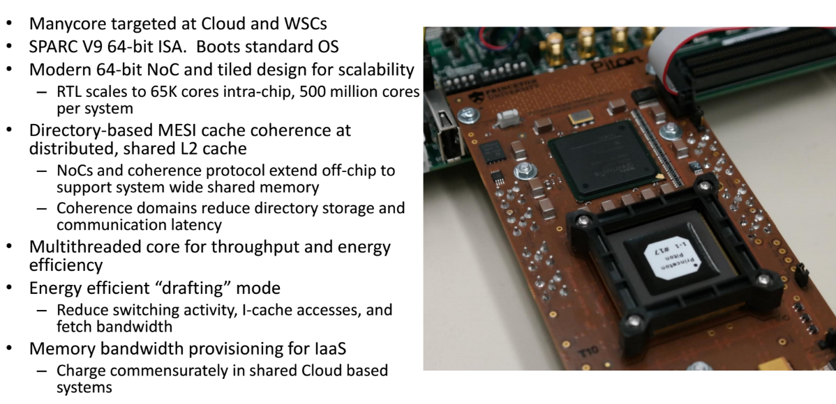
As seen in the architecture overview, this SPARC ISA, tile-based design is connected with a 64-bit on-chip network. The on-chip networks and coherence protocol extends off the chip, so the same interconnect is both on and off-chip, which, along with the “coherence domains” concept, allows for the system-wide shared memory.
The team is also targeting throughput and energy efficiency and accordingly, uses a multithreaded core with an energy efficient “drafting mode” on top, which cuts down on switching activity and instruction cache accesses. At its simplest, this core energy efficient drafting mode groups together similar or alike code into the multithreaded core and aligns execution points of threads to identical instructions.
At the center of the chip is the OpenSPARC T1 core, which provides a 6-stage in-order pipeline; 2-way multithreading for better throughput and to hide memory latency; L1 caches for instruction and data. The L2 cache structure is interesting as well. Here, distributed cache is shared by all the tiles (64KB slice per tile with 1.6MB aggregate cache per chip).
Other features of the L2 cache structure include 4-stage dual pipelines; 5-cycle hit latencies; an integrated directory cache; 64-byte line size capability and shared SRAM macros that extend between the two pipelines. As more becomes available about this chip in paper format, we expect more information on how this and the coherence domains interplay.
McKeown says OpenPiton is scalable to a half billion cores with configurable cache sizes and configurable NoC toplogy for further research.
The team has several chips in its labs now and is developing the OpenPiton open source release with RTL and testing tools, simulation infrastructure and FPGA synthesis capabilities. A side goal, McKeown says, is to target several FPGAs at different price points for comparison. If Hot Chips presentations were two hours we would still be holding on for more detail.
As it stands now, we will follow up with the Piton team later this year to see how different FPGAs change the performance and efficiency profiles (thus cost) and what any of the cloud vendors they’ve talked had to say about the ability to charge for memory bandwidth usage–a potential game changer of an option for both IaaS vendors and end users.

Be the first to comment