Nvidia made a lot of big bets to bring its “Pascal” GP100 GPU to market and its first implementation of the GPU is aimed at its Tesla P100 accelerator for radically improving the performance of massively parallel workloads like scientific simulations and machine learning algorithms. The Pascal GPU is a beast, in all of the good senses of that word, and warrants a deep dive that was not possible on announcement day back at the GPU Technology Conference.
We did an overview of the chip back on announcement day, as well as talking about Nvidia’s own DGX-1 hybrid server platform, which pairs two current Intel Xeon processors with eight of the Pascal-based Tesla cards to create a system that delivers 170 teraflops of half precision floating point performance, which is a huge performance jump for the hyperscale customers who are looking to run deep learning algorithms based on neural networks on larger datasets while at the same time boosting the overall performance of those algorithms. A few select customers are getting their hands on the Tesla P100 accelerators early, including the largest hyperscalers – Google, Facebook, and Baidu are probably at the front of the line – and a few supercomputer centers like Oak Ridge National Laboratory and the Swiss National Supercomputing Center.
There is plenty of time for the rest of the market to salivate over Pascal, which will ship in volume by the end of the year and which will be available in systems from IBM, Cray, Dell, and Hewlett Packard Enterprise by the first quarter of 2017. These and other server makers are ready to deploy Pascal Tesla P100 accelerators now or will soon be able to, and we think that Nvidia is simply not able to get enough of these new Pascal GPUs out of its fab partner, Taiwan Semiconductor Manufacturing Corp, to satisfy the demand of those top-end HPC and hyperscaler customers, much less a broader market. And that is why Nvidia is in no hurry to sunset its older “Kepler” and “Maxwell” GPU accelerator cards. The company is content to keep some of the Pascal GP100 GPUs to put into its own DGX-1 server appliances and sell them to deep learning researchers and newbies that will help expand its market, and then ramp up revenues when the Pascals are more widely available. If Nvidia can charge around $10,500 per Tesla P100 card, as we think it can do, because demand has outstripped supply, that is all the better for its top and bottom line.
Moreover, by launching the Pascal GPUs before they are shipping in volume, Nvidia can also blunt the inevitable attack that will be coming with Intel’s “Knights Landing” Xeon Phi parallel X86 processor, which has high bandwidth memory of a different style based on the Hybrid Memory Cube (HMC) technology that it co-developed with Micron Technology and which will ship in volume later this year, and the hybrid Xeon-FPGA chips it is forging, which will be shipping in prototype single-socket configurations to hyperscale and HPC customers this year and that will be available on a single die next year.
These are certainly interesting times in the systems space.
The Feeds And Speeds Of Pascal GP100
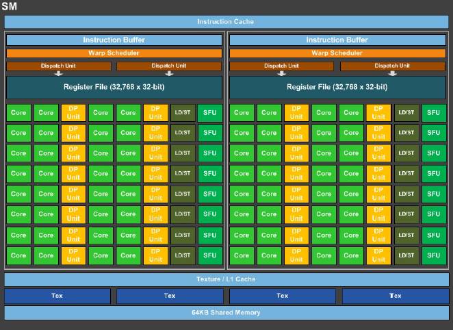
With Nvidia GPUs, the basic unit of compute is a 32-bit CUDA core and these cores are organized into streaming multiprocessors, or SMs, that gang up the cores with load/store units and special function units (SFUs) as well as double precision floating point math units, register files, warp schedulers, instruction buffers, L1 cache and 64 KB of shared memory around the whole shebang. With every generation of GPU, and even within generations of GPUs, Nvidia changes up the mix and capacities of these elements and sometimes adds new capabilities (like Hyper-Q and dynamic parallelism with the “Kepler” family of GPUs), but the basic architecture of Nvidia’s GPUs since it has been supplying Tesla coprocessors has been consistent. Here is what the Pascal SM looks like:
What is immediately obvious from this diagram is that the number of double precision math units in each SM is half that of the number of single precision CUDA cores, which means that at any given clock speed, the DP floating point performance in the die is precisely half that of the SP performance. With the prior Kepler and “Maxwell” generations of GPUs used in Tesla coprocessors, the ratio was one DP unit for every three SP cores, and this ratio was not a particularly useful one in terms of providing balanced price/performance.
While the 32-bit CUDA cores support 32-bit and half precision 16-bit processing by crunching a pair of 16-bit instructions at the same time (which effectively doubles the floating point operations per second on 16-bit datasets), the 64-bit DP units are not able to chew through two 32-bit or four 16-bit instructions in a single clock. When we suggested to Jonah Alben, senior vice president of GPU engineering at Nvidia, that it was a shame that these 64-bit units could not be used in such a manner, he said that the support for FP16 math required tweaks to the FP32 CUDA cores and that the register bandwidth would have been too limited to run FP16 instructions through both sets of elements at the same time. But it would be cool if it were possible to do this, and perhaps even cooler to be able to create a CUDA core that spoke FP16, FP32, and FP64 at the same time. That said, the Pascal GP100 GPU is the undisputed leader in both SP and DP performance among compute elements that are available today, so Nvidia knows what it is doing and the cost of a DP operation is now twice that of an SP operation, which is as things should be.
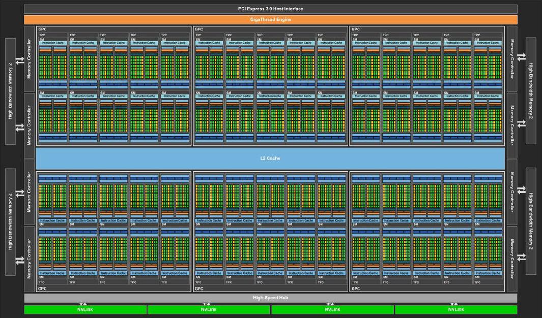
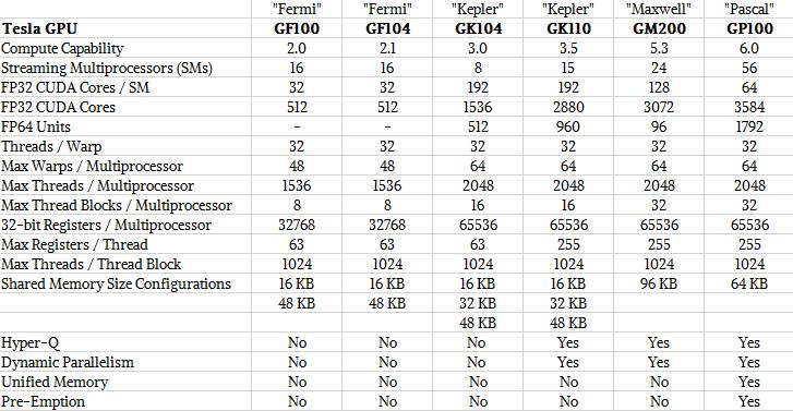
The other thing to notice about the Pascal SMs is that they have half the number of CUDA cores, and that means the shared memory and register files per SM has gone up. The ratio is twice as high as compared to the Maxwell SM, in fact. The Pascal GPU has up to 60 SMs, with only 56 being active in the GP100 variant of the chip, which helps Taiwan Semiconductor Manufacturing Corp get better yields on the chips because up to four of the SMs can be duds and Nvidia can still use it. Because of the increase in shared memory, registers, and warps (units for managing groups of threads) due to the larger number of SMs on the Pascal die, the chip can manage more threads in flight than its Kepler and Maxwell predecessors.
Just for review, here are how the capabilities of the last three generations of Tesla GPUs line up:
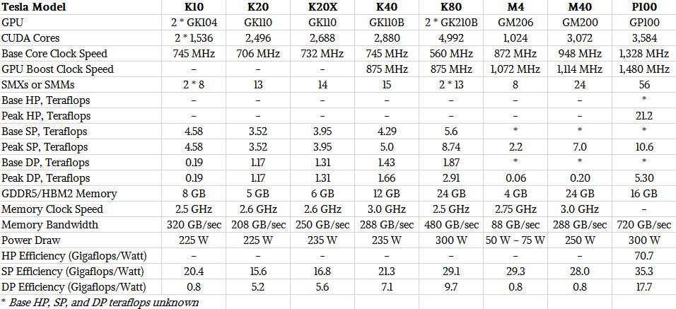
And for review, here are the feeds and speeds of the three generations of Tesla accelerator cards:
There are a number of other important architectural enhancements that accompany the Pascal GPU, at least for the high end implementation that is being used for the Tesla P100 accelerators. Alben, like other executives from Nvidia, was coy about how future Pascal GPUs and graphics cards might differ from the GP100 chip and the P100 card, but obviously there will be variants over the long haul. “We are not talking about unannounced products,” told The Next Platform, “but this architecture is a family and you should expect to see other products in this family that are tuned for different markets. As a for instance, you probably should not expect to see NVLink in other Pascal products because that is sort of specific to HPC.”
Given how the HPC and hyperscalers are keen on using NVLink to lash together the memories of multiple GPUs to do larger simulations and models in a single node, that would sort of undermine the need for a future Tesla P40 or double-whammy Tesla P80 card (if Nvidia could make one, which seems like a difficult engineering challenge). And it is not at all clear that Nvidia will make all members of the Pascal family with HBM2 stacked memory from its partner, Samsung, or will somehow be able to use GDDR5 frame buffer memory with the Pascal chip, much as it has done with the Keplers and the Maxwells.
“The P100 obviously has a lot of the technology packed in there,” Alben explained. “We were trying to think about building the best possible thing and just picking the best technologies, whatever they were. My general architectural philosophy is that Nvidia is about developing one common, core architecture and how we are able to service self-driving cars, HPC, deep learning, and gaming. The way we are able to service these many markets is that we find that right balance between a core design and then we get synergy and when we do X, then X actually helps us in other markets and it amplifies our strengths as a company. So for instance, with the Pascal architecture, we are doing pre-emption, and the motivation for that came from HPC customers, but it also benefits automotive, which has real-time workloads and GeForce as well. We find inspiration from one area and hopefully other areas get the benefits from that. Some things are specific investments for a specific market, like double precision. It doesn’t make sense for every customer to carry that FP64 load.”
The pre-emption feature was particularly tricky, said Alben, because stopping thousands of threads in flight and saving their state is no easy task. This Compute Preemption capability was not discussed in detail at the launch, but it has been detailed somewhat in this whitepaper on the Pascal architecture that has been released and our colleague, Chris Williams, over at our sister publication The Register, has done a good job explaining it, too. The Kepler architecture had a coarse-grained preemption, but even still when graphics and compute jobs were running in the same GPU, the long running compute jobs could monopolize resources on the GPU and cause visualization workloads or the operating system on the CPU side of a system to jitter. To get around this, programmers had to code their compute applications in small chunks that would finish relatively quickly. With the compute preemption in the Pascal GPU, the compute code can be as large and monolithic as developers want and they do not have to break it up to avoid this contention between compute and graphics, and that means both workloads can run on the same system at the same time. This is increasingly being done with GPU-based databases, like MapD, as well as for simulations that render models while creating them.
Unified memory is much improved with the Pascal architecture, too. The Fermi GPU architecture and its CUDA environment wrapped up the thread local memory, thread block shared memory and GDDR frame buffer memory into a unified address space. With CUDA 4, five years ago, Nvidia delivered unified virtual addressing, which allowed code running on the GPU to see the memory on both the GPU and the CPU as a virtual memory address space over the PCI-Express bus that the GPU cards hung off of. With CUDA 6, this virtual memory address space was extended in both directions over both the CPU and GPU, which radically simplified programming and data movement under the covers between the two memory regions, but the performance of this unified memory was limited because of the intricate synchronization that the Kepler and Maxwell GPUs had to do and because the memory space was limited to the size of the GPU’s frame buffer memory. With Pascal, Nvidia has boosted the virtual memory address space for unified memory to 49 bits, and now the virtual address space is big enough to wrap around both CPU and GPU memory. The new Pascal memory architecture also supports a new page faulting mechanism that automatically keeps the unified memory coherent across the CPUs and GPUs in the system node without programmers having to do any synchronization of data across those elements manually, and it works over PCI-Express and NVLink connections.
The last big change that comes with the Pascal architecture is the NVLink interconnect, which we will be drilling down into separately.
Add it all up, and Pascal makes substantial strides in delivering balanced GPU performance at different precision levels, high memory bandwidth, scalability across multiple GPUs thanks to NVLink, and much better virtual memory addressing. It will be interesting to see what Nvidia cooks up for the “Volta” GV100 GPU that is due in late 2017 or so. All that NVidia has hinted is that Volta will offer a little less than twice the single precision performance per watt as Pascal, which will be an impressive feat.



Don’t expect that most Pascal incarnations will have HBM2 there is a massive shortage in production on this which drives the price into astronomical spheres. So whatever comes till the end of 2016 will likely not feature it
I’m curious about this:
“The new Pascal memory architecture also supports a new page faulting mechanism that automatically keeps the unified memory coherent across the CPUs and GPUs in the system node without programmers having to do any synchronization of data across those elements manually, and it works over PCI-Express and NVLink connections.”
And the whitepaper doesn’t really clarify it.
Page faulting is one thing, and it sounds like there’s a hardware page walker. However, isn’t keeping the memory coherent going to be difficult on x86 without access to QPI? On POWER the CAPI interface is in the coherence domain so they’ll see the traffic and can participate, I assume. However, on x86, they won’t see the traffic and can’t be involved in keeping cache lines coherent, right?
I suppose one could hack it and mark the pages non-cacheable or something but performance will suck and it’ll be quite coarse grained compared to what they’re implying.
Any further details on this unified memory coherence on x86?
to author,
does it mean pascal has async compute capability like amd?
> With the prior Kepler and “Maxwell” generations of GPUs used in Tesla coprocessors, the ratio was one DP unit for every three SP cores,
Not exactly.
For Kepler, yes: K40s specs are 4.29 TFlops SP vs 1.43 TFlops DP, which is indeed a 1/3 ratio.
But for Maxwell, oh no no no. Specs for the M40 are 7 TFlops SP, 0.2 TFlops DP. That’s a *1/35* ratio. Which pretty much made the Maxwell generation useless for traditional compute. Lots of other advantages, though. But double-precision? Nah.
I was referring to the expected GM210 kicker to the unit used in the K40 and K80, which never saw the light of day and which, as far as I know, had the same 1 to 3 ratio for DP to SP.
How would Nvidia do 1:3 ratio with 128 FP32?
Too many of mistakes:
– GM200 is CC 5.2 not CC 5.3 (those are the embedded devices).
– Something stinks about the coherence over PCIe statement, I vaguely remember “software assist” mentioned curing one of the talks case in which it’s not on the same page as NVlink + CAPI.
– Same SP/DP ratio on Kepler and Maxwell!???
On a different note, while the HPC/tech reporting seems to be ecstatic about this sortof release, let’s see how will it look after ISC16.