

The workhorse of the datacenter, the Xeon E5 processor, is getting a bit stronger today and will be able to pull slightly heavier workloads through the datacenter with the launch of the “Broadwell” Xeon E5-2600 v4 processors.
The Broadwell Xeons are manufactured using Intel’s 14 nanometer chip processes, and constitute what is called a “tick” in its “tick-tock” chip evolution process. With a tick, Intel moves to smaller transistor sizes, which allows it to add more throughput to the chips, and with a tock it makes more substantial changes to the architecture and rolls them out on that now mature manufacturing process. Going forward beyond the future “Skylake” Xeon E5 v5 processors, expected perhaps in late 2017, Intel will be moving to a tick-tock-tock rhythm for its chips, stretching out its manufacturing process times for a bit since it is getting more difficult to do process shrinks as transistor wires are approaching the size of individual atoms. There is much debate on this, but we think it would be interesting to see the company move to an annual cadence for Xeon processor, which it might be able to do because it uses each process for a longer period of time.
The important thing for server buyers today is that Moore’s Law is providing more threads, more cores, and more L3 cache for applications to play in at prices that are more or less the same as the parts they replace in the line. Intel took the time to make some improvements in the microarchitecture of the Broadwell Xeons to help boost their single-threaded performance as well, keeping it on a track that has been fairly linear over the past decade when it was also radically boosting the number of cores. We will have more to say on this separately, and will do a thorough price/performance analysis of the Broadwell chips and the platforms that use them. But to start, we want to tell you about the new chips.
As has been the case for the past several Xeon E5 generations, there are a slew of new processors covering all kinds of use cases where core counts, clock speeds, caches, and costs are all individual variables that customers want to dial up to meet their workload needs. Long gone are the days when there were just a few SKUs and companies had to make do. With the Broadwell Xeon E5 chips, Intel has created 24 standard parts, plus two with very high core counts that are not on the official price list, and one more aimed at workstations. There are likely another set of chips that is has made custom for hyperscalers, cloud builders, and HPC centers, as it has done in past years to try to meet the needs of these high-end customers while keeping the competition at bay. (We do not know the precise number of custom Broadwell Xeon E5 parts, but we do know there is one with very high clock speeds that is designed explicitly for high frequency trading applications.)
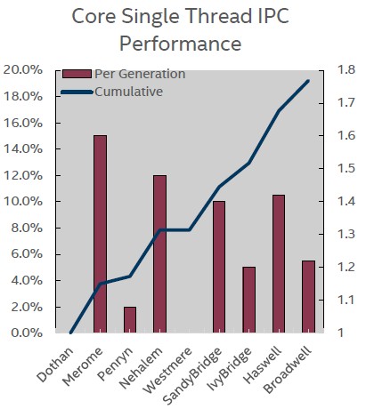
“Broadwell is a tick, but it includes a robust set of microarchitectural changes that deliver about a 5.5 percent improvement in single thread performance for the cores, separate from core count and frequency changes,” Chris Gianos, the chip engineer who has steered the development of the Haswell Xeon E5 v3, the Broadwell Xeon D-1500, and the Haswell Xeon E7 v3, tells The Next Platform. “This is just take your work, run it through, and it now takes about 5.5 percent fewer clock cycles to get the work done on a Broadwell thread than it did on a Haswell thread.”
The Broadwell Xeon E5s also have more cores for any given spot in the Xeon processor lineup, with the top-bin part sporting 22 active cores compared to 18 active cores for the equivalent Haswell Xeon – which is a 22 percent increase in core count. So it is not much of a surprise, then, that on early benchmark tests, the Broadwells are showing performance increases in the middle 20 percent range compared to the Haswells that they replace and a mean increase of about 27 percent across a spectrum of workloads.
The good news is that the Broadwell E5 chips plug into the same LGA 2011 socket that was created specifically for the Haswell E5 chips and that is also known as Socket R3. (The Socket R2 used with the prior “Sandy Bridge” and “Ivy Bridge” Xeons, which were v1 and v2 generations, had the same physical shape but cannot take the Haswell or Broadwell chips because their pins are used for different signaling and power purposes.) Most companies will not actually upgrade the Haswell processors in an existing system to a Broadwell processor, but the compatibility is important for system vendors, which want to get two generations out of a system design before having to redo their motherboards and go through qualifications for software stacks all over again. With the tick-tock-tock rhythm that Intel will be deploying going forward, they could get three generations of chips out of a single system eventually, but Skylake’s “Purley” platform – meaning the combination of the processor, chipsets, and motherboards from Intel – could be the first to span three Xeon chips, perhaps from 2017 through 2020. The current platform supporting Haswell and Broadwell Xeon E5 processors is code-named “Grantley.”
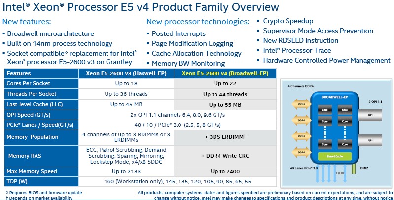
Technically speaking, the chips that Intel is announcing today are the Broadwell-EP line, with the add-on being short for “efficient performance” and designating that this is the workhorse chip covering the widest possible application ranges. Each Broadwell core has 32 KB of L1 data cache, 32 KB of L1 instruction cache, and 256 KB of L2 cache; the cores also have Intel’s implementation of simultaneous multithreading, called HyperThreading, which presents two virtual cores for every physical core in the chip and can boost performance on certain workloads. Each core also has a 2.5 MB L3 cache segment associated with it, and these are glommed together to make a shared L3 cache that spans all of the cores. In the case of the Broadwell chips, that adds up to a maximum of 55 MB of L3 cache, a 22 percent increase over the 45 MB of L3 cache in the largest Haswell Xeon E5.
There is not actually one Broadwell-EP chip, but rather three, which Intel ranks by low, medium, and high core count. (The Sandy Bridge, Ivy Bridge, and Haswell chips also were really three different chips with varying number of cores and caches.) The high core count variant is the one that is pushing the architectural limits, and here is what it looks like:
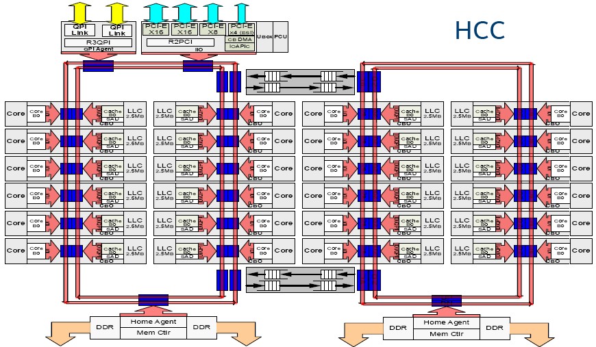
“In the HCC chips, there is no longer an asymmetric core count in the right hand column; it is more of a rectangular grid,” says Gianos. “The lower core SKUs of the HCC chip have the cores taken out symmetrically from all of the columns so things stay relatively balanced – you want one memory controller per ring, the same number of cores per ring, and so on. It feels a little bit more balanced, but honestly no one has been able to show a measurable imbalance with Haswell, but people like the symmetry,” he adds with a laugh.
To increase its chip yields, Intel is only activating a maximum of 22 of the 24 cores on the HCC chip in the product line, and the variants with 20 or 22 cores fall somewhere between standard and custom parts in the scheme of Xeon things. Practically speaking, the real top-bin Broadwell Xeon E5 v4 parts have 16 or 18 cores, compared to 14 cores for the prior generation of Haswell Xeon E5 v3 chips.
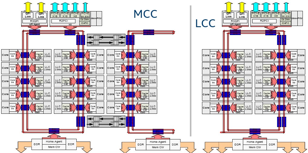
The medium core count variant of the chip has a maximum of fifteen cores and two rings and is available with ten, twelve, or fourteen active cores. The low core count variant has a maximum of ten cores on the die and is available with four, six, or eight cores that are accessible by applications. Again, the spare cores are added so that as Intel tests the chips those that might have two cores not working right but all other elements are fine can be sold instead of thrown into the scrap heap. This is a smart way to increase yields, and all processor makers do it these days. (Well, the few that are left, anyway.)
If you are keeping score, the HCC variant of the Broadwell Xeon E5 has 7.2 billion transistors, the MCC variant has 4.7 billion transistors, and the LCC variant has 3.2 billion transistors. The Haswell-EX Xeon E7 processor from last year had 5.7 billion transistors, and the equivalent HCC, MCC, and LCC parts in the Haswell generation had 5.6 billion, 3.8 billion, and 2.6 billion transistors, respectively, so the shrink from 22 nanometers to 14 nanometers gave Intel about 23 percent more wires in the LCC and MCC parts and about 28.5 percent more wires in the HCC parts.
“The Xeon architecture is certainly capable of building any combination of cache and core count that we desire and it has been since Haswell,” says Gianos.
By the way, that ring interconnect that came out with the Sandy Bridge and Ivy Bridge Xeon E5s ran at the same speed as the cores, rising in turbo mode and dropping back down to normal mode as they could. (Prior “Nehalem” and “Westmere” Xeons could turbo their cores, but the “uncore” interconnect and L3 caches ran at a fixed speed, which was not optimal.) With Haswell, uncore frequency scaling was introduced, which meant that the cores could run at a different speed from the interconnect ring and the L3 caches. On Broadwell, like Haswell, the ring and L3 caches can run at frequency that is different from the cores, and by and large the ring runs in the middle 2 GHz range and turbo up to the high 2 GHz range when there is more demand for bandwidth and it can scale down to near 2 GHz when more speed (which creates heat) is not needed.
The QuickPath Interconnect, or QPI, bus that links multiple processors together remains the same on the Broadwell Xeon E5s as it was with the Haswells. The fastest versions with the most cores have QPI links that run at 9.6 GT/sec (that’s gigatransfers per second), while others with fewer cores run at 6.4 GT/sec or 8.6 GT/sec. The Xeon E5 chips implement a pair of QPI links to create a NUMA system that shares memory across two sockets. As with the Haswells, the Broadwells have a maximum of 40 PCI-Express lanes coming off a pair of chips, which is controlled by on-die PCI-Express controllers and which is used to hang peripherals off the processing complex.
The one big change with the Broadwell E5s is that the chips now support CRC error correction on writes to the DDR4 memory sticks used with the processors. Also, in machines that only hang two memory sticks on each memory channel, the maximum memory speed has been boosted to 2.4 GHz, up from 2.13 GHz with the Haswells. However, those who want to hang three memory sticks on each channel to boost the memory capacity will have to run the DDR4 memory at 1.6 GHz. The Broadwell chips have a total of four memory channels implemented across their on-die controllers.
Further on the memory front, the Transactional Synchronization Extensions (TSX), which were etched into the Haswell cores to give it support for transactional memory was not activated a year and a half ago in the Haswell Xeon E5s because of a bug. This bug was fixed with the Haswell Xeon E7 and Broadwell Xeon-D processors last year, and TSX is finally being activated on the Broadwell Xeon E5s. TSX removes the locking mechanisms that keep threads from manipulating the same data in main memory and lets all threads complete all of their work in parallel. In a normal system, when data is used by a thread, it is locked so no other thread can touch it, and that means other threads can stall even if they are only reading the data. By eliminating the locks at the front end and doing checks only after threads are done with their work, applications can run a lot faster.
Frank Jensen, performance marketing manager at Intel, told us last summer when the Haswell Xeon E7 processors were launched that on certain HPC workloads, TSX delivered about a 40 percent boost in performance on clusters. Intel’s tests on SAP’s HANA in-memory database using TSX showed about a 2X boost from TSX alone, and then moving from 15-core Ivy Bridge E7s running SAP HANA SP8 to 18-core Haswell E7s running HANA SP9 and then turning on TSX boosted performance by 5.9X. The Sybase database is showed a 1.2X boost from TSX, and MySQL, Oracle 12c, and Microsoft SQL Server have all been tweaked to take advantage of the TSX feature and now will be able to use it on the Xeon E5.
The Feeds And Speeds
Intel organizes the Broadwell Xeon E5 processors in a number of different classes, not just according to the bulk number of cores on the design. These classes vary in terms of core counts, cache sizes, QPI speeds, memory speeds, and whether or not they support Turbo Boost and HyperThreading. Take a look:
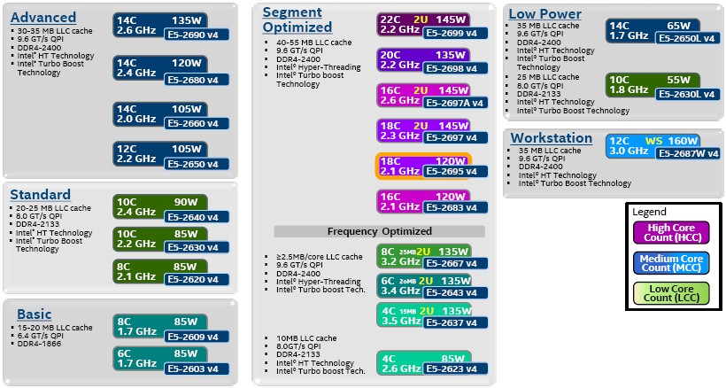
There are 22 chips that are standard parts, plus the two top-bin parts that are for the most part aimed at HPC shops looking to cram the most cores possible in a socket. In addition to these chips shown in the chart above, there are five Broadwell Xeon E5s that have been designed for long life and extended warranties, which is necessary for network and storage equipment that has a much longer shelf life than a typical server in a datacenter.
The one thing that this chart above does not show is specific feeds and speeds and pricing, so we have built a summary table for you below:
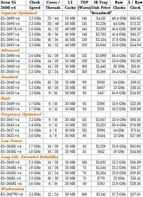
As you can see, generally speaking, the more cores you have on the die and the more performance you can express through aggregate clocks, the more the Broadwell Xeon E5 chip costs. Intel did not initially provide pricing for the top two SKUs, a practice it started with the Haswell Xeon E5s in September 2014, but changed its mind and has actually published the prices for these chips, which are pricey indeed. (We have updated our table to reflect this change.)
As we do in our initial rudimentary analysis for every Intel chip launch, we have counted up the aggregate clocks in each chip to get a reckoning of relative performance within the Xeon E5 generation, which is shown in the far right column. We have a much more sophisticated price/performance analysis in the works that takes into account the Xeon line from the transformational Nehalem-EPs launched in March 2009 up through the current Broadwell-EPs.
What we can say generally is that SKU for SKU, customers are getting a reasonable bump in performance for a tick, and they are probably not going to pay a lot for it – and perhaps nothing at all if they negotiate hard either with Intel (if they buy chips directly) or with their server maker (if they do not). Here is the initial comparison that Intel is showing for various workloads, pitting the Broadwell Xeon E5 against its Haswell predecessor:
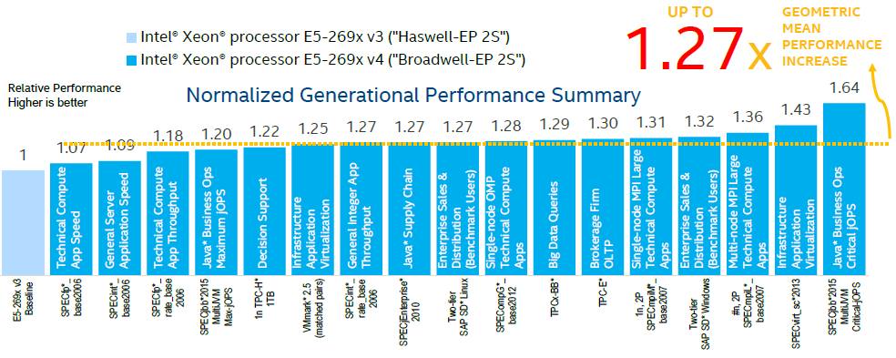
In the chart above, Intel is comparing the performance at a server level with two sockets populated with processors. The tests are not run on the same processors each time, so the comparisons are not perfect. But this gives a general feel for how the performance will be.
In addition to a more thorough price/performance analysis, we will also be looking at how Intel is positioning the Broadwell Xeon E5 processors against its prior generations of machines and competing Power-based systems from IBM and taking a look at how Intel has managed to boost performance over the past decade and what its prospects are for the immediate future. Finally, we will also be drilling down into some of the new features that have been added to the Broadwell cores to accelerate virtual machines and hypervisors, security algorithms, and HPC workloads. Stay tuned.

To Cure Iron Anemia With SYCL, Intel Buys Codeplay
Intel doesn’t want to just create a rival to the CUDA programming model and library stack so it can better compete against Nvidia in the GPU compute market. With oneAPI, it wants to create an open ecosystem that includes a programming framework, called oneAPI and largely based on the SYCL …
Keeping Pace In A Fast-Moving AI Space
During the Intel AI Summit earlier this month where the company demonstrated its initial processors for artificial intelligence training and inference workloads, Naveen Rao, corporate vice president and general manager of the Artificial Intelligence Products Group at Intel, spoke about the rapid pace of evolution in the AI space that …

Argonne Aurora A21: All’s Well That Ends Better
When it comes to a lot of high performance computing systems we have seen over the decades, we are fond of saying that the hardware is the easy part. This is not universally true, and it certainly has not been true for the “Aurora” supercomputer at Argonne National Laboratory, the …
Xeon E5 2600 EP Ivy v2 & Haswell v3 full run by core count, power dissipation and frequency distribution on broker channel volume data.
26xx EP v2 4 Core 17.22%
26xx EP v3 4 Core 05.49%
26xx EP v2 6 Core 21.71%
26xx EP v3 6 Core 33.47%
26xx EP v2 8 Core 25.43%
26xx EP v3 8 Core 21.62%
26xx EP v2 10 Core 26.62%
26xx EP v3 10 Core 18.23%
26xx EP v2 12 Core 09.00%
26xx EP v3 12 Core 09.74%
26xx EP v3 14 Core 07.68%
26xx EP v3 16 Core 01.87%
26xx EP v3 18 Core 02.23%
2600 EP v2 % Power Dissipation
50w < 01.00%
70w 00.17%
80w 32.29%
95w 27.75%
115w 16.98%
120w 00.07%
130w 21.47%
150w 01.26%
2600 EP v3 % Power Dissipation
50w 00.02%
55w 00.07%
65w 00.07%
75w 00.08%
85w 42.93%
90w 05.87%
105w 17.98%
120w 11.03%
135w 14.29%
145w 05.86%
160w 01.79%
2600 EP v2 % Frequency Distribution GHz
1.6 00.00%
1.7 00.13%
1.8 06.22%
1.9 00.05%
2.0 08.64%
2.1 09.24%
2.2 07.64% – 1.6 to 2.2 GHz = 31.92%
2.3 00.00%
2.4 04.46%
2.5 14.48%
2.6 20.20% – 2.3 to 2.6 GHz = 39.14%
2.7 04.45%
2.8 06.22%
2.9 00.00%
3.0 06.36%
3.1 00.00%
3.2 00.00%
3.3 04.01%
3.4 01.26%
3.5 06.64% – 2.7 to 3.5 GHz = 28.95%
2600 EP v3 % Frequency Distribution GHz
1.6 07.59%
1.7 00.00%
1.8 00.19%
1.9 08.12%
2.0 02.31%
2.1 00.00%
2.2 00.11% – 1.6 to 2.2 GHz = 18.32%
2.3 16.74%
2.4 29.14%
2.5 03.55%
2.6 17.83% – 2.3 to 2.6 GHz = 62.27%
2.7 00.00%
2.8 01.31%
2.9 00.02%
3.0 02.72%
3.1 01.79%
3.2 02.84%
3.3 00.00%
3.4 02.97%
3.5 02.78% – 2.7 to 3.5 GHz = 14.42%
Mike Bruzzone, Camp Marketing
Hi Timothy,
Thanks for writing this great article.
We have been using two Ivy Bridge 10C E5-2690V2 3.0Ghz processors with XenServer supporting virtual desktop workloads. The virtual desktops run Autodesk Revit, which is single threaded in many of its operations. I am evaluating new servers with Haswell and Broadwell procs but due to the thermal constraints, I can no longer get a 10 core / 3 GHz processor in any form factor under a 4U server. Currently we have 1U servers so we are not going to 4U. I am trying to determine if a 2.6Ghz Haswell or Broadwell core can perform as well as a 3GHz Ivy Bridge.
Thanks for any insight you have on this!
Richard
Try looking at the charts I built here:
https://www.nextplatform.com/2016/04/04/xeon-bang-buck-nehalem-broadwell/
Shows relative performance based on IPC and aggregate clocks across the past many generations.
Will do. Thanks for responding, Timothy!
Richard
I don’t agree. Read:
http://www.avadirect.com/blog/intel-core-vs-xeon-which-is-best/ Friendly, Claudie